While incredibly powerful, thin film deposition is not a simple process and comes with significant technical challenges. The primary disadvantages revolve around the difficulty of controlling the film's physical properties, ensuring it adheres properly to the surface, and managing the high costs and complexities associated with scaling the process for production.
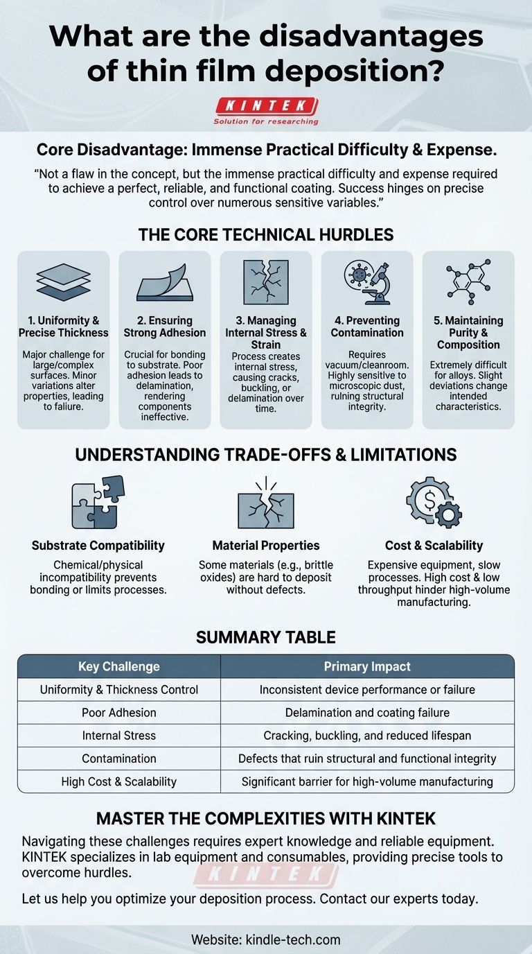
The core disadvantage of thin film deposition is not a flaw in the concept itself, but the immense practical difficulty and expense required to achieve a perfect, reliable, and functional coating. Success hinges on precise control over numerous sensitive variables.
The Core Technical Hurdles of Thin Film Deposition
The theoretical benefits of thin films are often shadowed by the practical challenges of creating them. These hurdles are the true disadvantages of the process.
Challenge 1: Achieving Uniformity and Precise Thickness
Achieving a perfectly uniform film across an entire surface, especially a large or complex one, is a major challenge.
Even minor variations in thickness can drastically alter a film's optical, electrical, or mechanical properties, leading to device failure or inconsistent performance.
Challenge 2: Ensuring Strong Adhesion
A film is useless if it doesn't stick to the underlying material, known as the substrate.
Poor adhesion can lead to delamination, where the film peels or flakes off. This is a critical failure mode that renders the component ineffective.
Challenge 3: Managing Internal Stress and Strain
The deposition process itself can create internal stress within the thin film.
This built-in strain can cause the film to crack, buckle, or delaminate over time, severely compromising its integrity and the function of the final product.
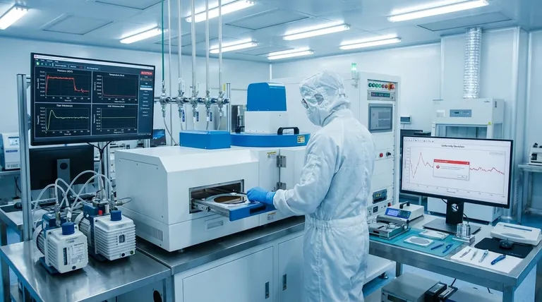
Challenge 4: Preventing Contamination
Thin film deposition often requires vacuum or cleanroom environments because the process is highly sensitive to contamination.
Even microscopic dust particles or residual gas molecules can create defects in the film, ruining its structural integrity and functional properties.
Challenge 5: Maintaining Purity and Composition
For films made of alloys or compound materials, maintaining the precise chemical composition and purity is extremely difficult.
Slight deviations from the target composition can fundamentally change the film's intended characteristics, making this a constant process control challenge.
Understanding the Trade-offs and Limitations
Beyond the direct technical hurdles, there are broader strategic disadvantages to consider, primarily centered on compatibility and cost.
The Constraint of Substrate Compatibility
Not every film material can be successfully deposited onto every substrate.
Chemical or physical incompatibility between the film and the substrate can prevent proper bonding, limit the process window, or create excessive stress, forcing costly changes in materials or design.
The Challenge of Material Properties
Some materials that would be ideal for a thin film are inherently difficult to work with. For example, certain brittle oxides can be challenging to deposit without introducing cracks or defects.
This means the ideal material for an application may not be practical to implement as a thin film, forcing engineering compromises.
The Reality of Cost and Scalability
The equipment needed for high-quality thin film deposition is expensive, and the processes can be slow.
This combination of high cost and low throughput makes scaling up from laboratory research to high-volume manufacturing a significant financial and logistical disadvantage.
Is Thin Film Deposition Right for Your Application?
Choosing this technology requires weighing its unique capabilities against its inherent difficulties. The right choice depends entirely on your project's primary goal.
- If your primary focus is achieving novel properties for high-performance devices (e.g., semiconductors, advanced optics): The technical challenges are a necessary and justifiable cost for creating functionality that bulk materials cannot provide.
- If your primary focus is improving a product with a cost-effective coating: You must carefully evaluate whether the complexities of adhesion, uniformity, and high capital cost are manageable within your budget.
Ultimately, successfully leveraging thin film deposition depends on your ability to master and control its demanding and sensitive process variables.
Summary Table:
| Key Challenge | Primary Impact |
|---|---|
| Uniformity & Thickness Control | Inconsistent device performance or failure |
| Poor Adhesion | Delamination and coating failure |
| Internal Stress | Cracking, buckling, and reduced lifespan |
| Contamination | Defects that ruin structural and functional integrity |
| High Cost & Scalability | Significant barrier for high-volume manufacturing |
Master the complexities of thin film deposition with KINTEK.
Navigating the challenges of thin film processes—from achieving perfect uniformity to managing high costs—requires expert knowledge and reliable equipment. KINTEK specializes in lab equipment and consumables, providing the precise tools and support needed to overcome these hurdles. Whether you're developing high-performance semiconductors or advanced optical coatings, our solutions help you control critical variables and ensure successful outcomes.
Let us help you optimize your deposition process. Contact our experts today to discuss your specific application and discover how KINTEK can enhance your laboratory's capabilities and efficiency.
Visual Guide
Related Products
- Aluminized Ceramic Evaporation Boat for Thin Film Deposition
- Tungsten Evaporation Boat for Thin Film Deposition
- Electron Beam Evaporation Coating Oxygen-Free Copper Crucible and Evaporation Boat
- Molybdenum Tungsten Tantalum Evaporation Boat for High Temperature Applications
- HFCVD Machine System Equipment for Drawing Die Nano-Diamond Coating
People Also Ask
- What are the applications of thin films deposition? Unlock New Possibilities for Your Materials
- Why are high-purity ceramic boats used for lignin activation? Ensure Purity & Thermal Stability
- What are thin films deposited by evaporation? A Guide to High-Purity Coating
- What is thin film deposition? Unlock Advanced Surface Engineering for Your Materials
- Why is an alumina boat and Ti3AlC2 powder bed necessary for Ti2AlC sintering? Protect MAX Phase Purity


