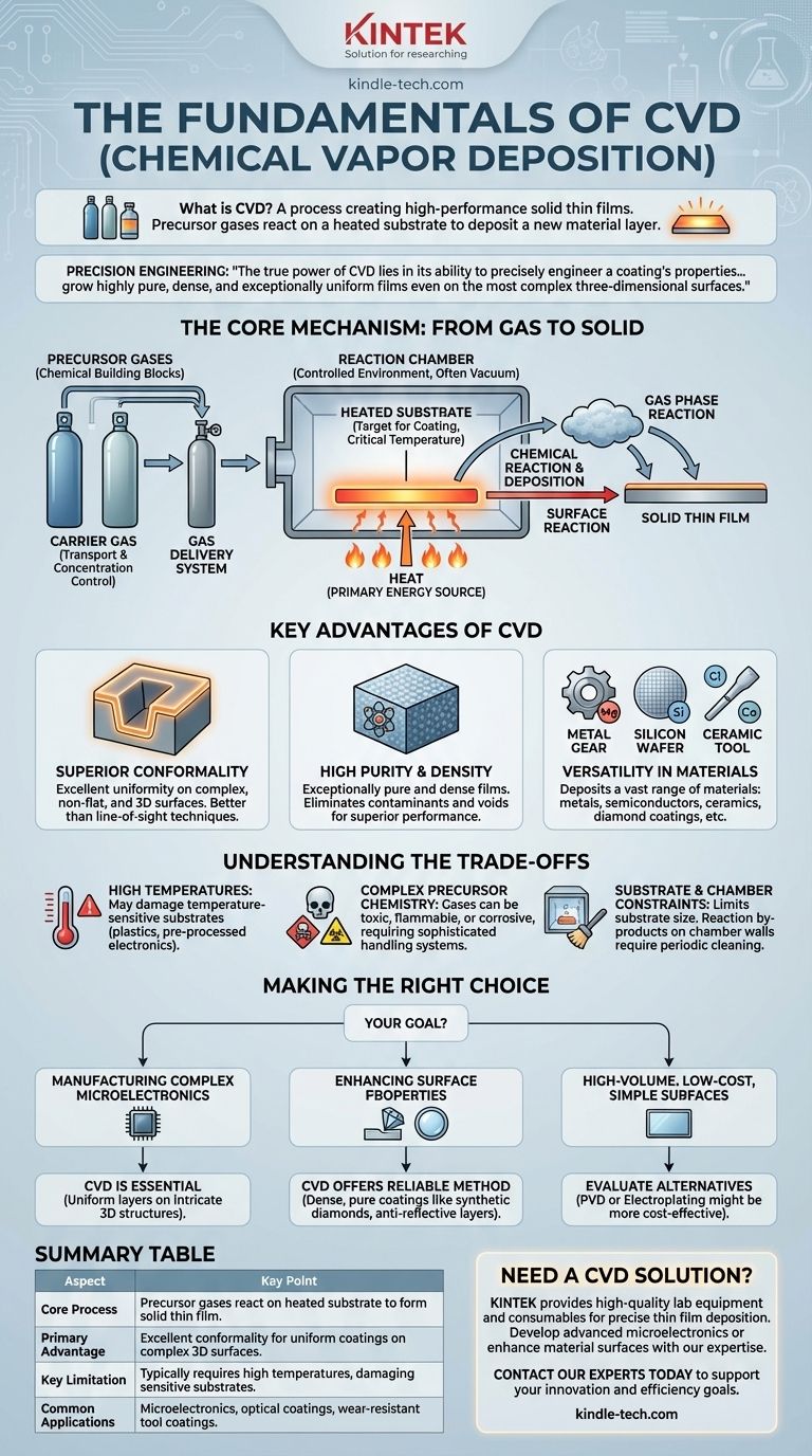
At its core, Chemical Vapor Deposition (CVD) is a process used to create high-performance solid thin films on a substrate. It achieves this by introducing precursor gases into a reaction chamber where, under controlled heat and pressure, they undergo a chemical reaction and deposit a new material layer onto the target surface. This method is fundamental to manufacturing in industries ranging from electronics to optics.
The true power of CVD lies not just in depositing a coating, but in its ability to precisely engineer that coating's properties. By manipulating gas chemistry, temperature, and pressure, you can grow highly pure, dense, and exceptionally uniform films even on the most complex three-dimensional surfaces.
The Core Mechanism: From Gas to Solid
To understand CVD, you must first understand its constituent parts and how they interact. The entire process is a carefully controlled chemical reaction happening within a contained environment.
The Role of Precursor Gases
Precursor gases are the chemical building blocks of the final film. They are carefully selected gases that contain the elements you wish to deposit.
These gases are delivered into the reaction chamber using a gas delivery system, often mixed with a carrier gas (like nitrogen or hydrogen) that helps transport them and control their concentration.
The Reaction Chamber and Substrate
The reaction chamber is a sealed vessel, often under vacuum, that contains the entire process. It provides the controlled environment necessary for the chemical reactions to occur predictably.
Inside this chamber is the substrate, which is the material or component that will be coated. The substrate is heated to a specific, critical temperature to facilitate the deposition.
The Critical Role of Energy
Heat is the primary energy source that drives the CVD process. Applying heat to the substrate and the chamber does two things: it provides the thermal energy needed to break chemical bonds in the precursor gases and enables the subsequent reactions that form the solid film.
The precise temperature is one of the most critical parameters, directly influencing the deposition rate and the quality, purity, and structure of the final film.
The Two Reaction Pathways
Once energized, the precursor gases form the solid film in one of two ways. They can either react directly on the hot substrate surface, or they can react in the gas phase above the substrate to form an intermediate chemical species which then deposits onto the surface.
Key Advantages of the CVD Process
CVD is not just one method among many; its unique characteristics make it indispensable for certain high-value applications.
Superior Conformality
The standout benefit of CVD is its excellent conformality. Because the precursor gases can flow and react on all exposed surfaces, CVD can create a perfectly uniform coating over complex, non-flat, and three-dimensional structures.
This is a significant advantage over line-of-sight techniques like Physical Vapor Deposition (PVD), which can create thin or incomplete coatings in trenches and on the "shadowed" sides of a feature.
High Purity and Density
The nature of the chemical reaction allows for the creation of films that are exceptionally pure and dense. By carefully controlling the input gases and eliminating contaminants within the vacuum chamber, the resulting solid material is free of voids and impurities that can degrade performance.
Versatility in Material Deposition
The CVD process is remarkably versatile. By changing the precursor gases, you can deposit a vast range of materials, including metals, semiconductors (like silicon), and ceramics (like silicon nitride). This flexibility is why it's used for everything from computer chips and optical lenses to synthetic diamond coatings on cutting tools.
Understanding the Trade-offs
No technology is without its limitations. Being an effective technical advisor means recognizing the constraints of a process.
The Need for High Temperatures
CVD typically requires elevated temperatures to drive the chemical reactions. This can be a significant limitation, as the required heat may damage or alter the properties of temperature-sensitive substrates, such as certain plastics or pre-processed electronic components.
Complexity of Precursor Chemistry
The gases used as precursors can be highly toxic, flammable, or corrosive. This necessitates sophisticated and expensive gas delivery and exhaust handling systems to ensure safety and environmental compliance. Managing this complex chemistry is a major operational consideration.
Substrate and Chamber Constraints
The process is contained within a reaction chamber, which limits the size of the substrate that can be coated. Furthermore, the chemical byproducts of the reaction can deposit on the chamber walls, requiring periodic cleaning cycles that impact manufacturing throughput.
Making the Right Choice for Your Goal
The decision to use CVD must be based on a clear understanding of your technical and commercial objectives.
- If your primary focus is manufacturing complex microelectronics: CVD is essential for its ability to create uniform, conformal layers on the intricate 3D structures found in modern computer chips.
- If your primary focus is enhancing surface properties like hardness or clarity: CVD offers a reliable method to grow dense, pure coatings like synthetic diamonds on tools or anti-reflective layers on optical glass.
- If your primary focus is high-volume, low-cost coating on simple, flat surfaces: You should evaluate whether the precision of CVD is truly necessary, as alternative methods like PVD or electroplating might be more cost-effective.
Ultimately, Chemical Vapor Deposition is a cornerstone of modern materials engineering, enabling the creation of advanced materials that would otherwise be impossible to produce.
Summary Table:
| Aspect | Key Point |
|---|---|
| Core Process | Precursor gases react on a heated substrate to form a solid thin film. |
| Primary Advantage | Excellent conformality for uniform coatings on complex 3D surfaces. |
| Key Limitation | Typically requires high temperatures, which can damage sensitive substrates. |
| Common Applications | Microelectronics, optical coatings, wear-resistant tool coatings. |
Need a CVD solution tailored to your lab's specific requirements?
KINTEK specializes in providing high-quality lab equipment and consumables for precise thin film deposition. Whether you are developing advanced microelectronics or enhancing material surfaces, our expertise and reliable products can help you achieve superior results.
Contact our experts today to discuss how we can support your laboratory's innovation and efficiency goals.
Visual Guide
Related Products
- CVD Diamond Dressing Tools for Precision Applications
- Multi Heating Zones CVD Tube Furnace Machine Chemical Vapor Deposition Chamber System Equipment
- CVD Diamond Domes for Industrial and Scientific Applications
- CVD Diamond for Thermal Management Applications
- Chemical Vapor Deposition CVD Equipment System Chamber Slide PECVD Tube Furnace with Liquid Gasifier PECVD Machine
People Also Ask
- Does the chemical vapor deposition be used for diamonds? Yes, for Growing High-Purity Lab Diamonds
- What are the disadvantages of CVD diamonds? Understanding the trade-offs for your purchase.
- What color diamonds are CVD? Understanding the Process from Brown Tint to Colorless Beauty
- What is chemical vapor deposition of diamond? Grow High-Purity Diamonds Atom-by-Atom
- Can CVD diamonds change color? No, their color is permanent and stable.


