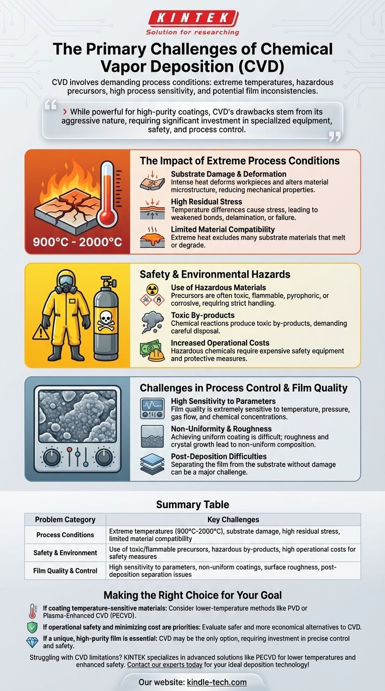
The primary challenges of Chemical Vapor Deposition (CVD) are rooted in its demanding process conditions. Key problems include the necessity for extremely high temperatures, the use of toxic or flammable precursor materials, significant process sensitivity, and potential inconsistencies in the final film quality. These factors create considerable safety, material compatibility, and operational hurdles.
While an exceptionally powerful technique for creating high-purity, high-performance coatings, the fundamental drawbacks of CVD stem from its aggressive chemical nature. This requires a significant investment in specialized equipment, safety protocols, and process control to mitigate risks to both the substrate and the operator.
The Impact of Extreme Process Conditions
The most significant limitations of CVD often arise from its reliance on high temperatures, which can range from 900°C to 2000°C. This thermal energy is necessary to drive the chemical reactions, but it also introduces several problems.
Substrate Damage and Deformation
Such intense heat can easily deform the workpiece or substrate being coated.
This high-temperature exposure can also alter the microstructure of the substrate material, potentially reducing its mechanical properties and overall integrity.
High Residual Stress
The significant temperature difference between the deposition process and room temperature can lead to high residual stress within the coating and at the interface with the substrate.
This stress can weaken the bond between the coating and the substrate, sometimes leading to delamination or failure.
Limited Material Compatibility
The extreme heat severely limits the types of materials that can be used as substrates.
Many materials cannot withstand the required temperatures without melting, deforming, or degrading, making CVD unsuitable for a wide range of applications.
Safety and Environmental Hazards
CVD relies on volatile precursor chemicals to supply the deposition material. The nature of these chemicals is a major source of concern.
Use of Hazardous Materials
Many of the source materials (precursors) and reactive gases used in CVD are highly toxic, flammable, pyrophoric, or corrosive.
This necessitates careful material handling, storage, and a robust system design to prevent leaks and ensure operator safety, which is a lesser concern in processes like Physical Vapor Deposition (PVD).
Toxic By-products
The chemical reactions that occur during deposition often produce toxic by-products. These must be handled and disposed of carefully, making the process less environmentally friendly than some alternatives.
Increased Operational Costs
The hazardous nature of the chemicals requires additional investment in safety and protective equipment. This, combined with the high cost of the CVD equipment itself, can make the process expensive to implement and operate safely.
Challenges in Process Control and Film Quality
Achieving a perfect, uniform coating with CVD requires precise management of a complex interplay of factors.
High Sensitivity to Parameters
The quality of the final film is extremely sensitive to process parameters like temperature, pressure, gas flow rates, and chemical concentrations.
If any of these factors are not controlled with high precision, it can result in a poor-quality film or even a complete failure of the deposition process.
Non-Uniformity and Roughness
It can be challenging to deposit a perfectly uniform film across a large substrate, particularly with complex materials like graphene.
Furthermore, the surface of a CVD coating often has a roughness that evolves with the film's thickness, and its grain structure can exhibit a non-uniform composition due to the crystal growth process.
Post-Deposition Difficulties
For some applications, such as producing freestanding graphene sheets, separating the deposited film from the catalyst substrate without causing damage or introducing impurities is a significant technical challenge.
Making the Right Choice for Your Goal
Ultimately, the decision to use CVD depends on balancing its powerful capabilities against its significant drawbacks.
- If your primary focus is coating temperature-sensitive materials: Standard high-temperature CVD is unsuitable, and you should prioritize lower-temperature methods like PVD or Plasma-Enhanced CVD (PECVD).
- If your primary focus is operational safety and minimizing cost: The hazardous materials and specialized equipment required for CVD demand careful consideration of alternatives that may offer a safer and more economical process.
- If your primary focus is creating a unique, high-purity film that demands it: CVD may be the only viable option, but success requires investing heavily in precise process control and rigorous safety protocols.
Understanding these inherent limitations is the first step toward selecting the right deposition technology for your specific application.
Summary Table:
| Problem Category | Key Challenges |
|---|---|
| Process Conditions | Extreme temperatures (900°C-2000°C), substrate damage, high residual stress, limited material compatibility |
| Safety & Environment | Use of toxic/flammable precursors, hazardous by-products, high operational costs for safety measures |
| Film Quality & Control | High sensitivity to parameters, non-uniform coatings, surface roughness, post-deposition separation issues |
Struggling with CVD limitations for your lab's coating needs? KINTEK specializes in lab equipment and consumables, offering advanced solutions like Plasma-Enhanced CVD (PECVD) systems that operate at lower temperatures with enhanced safety. Our expertise helps you achieve high-purity films without the typical CVD drawbacks. Contact our experts today to find the ideal deposition technology for your specific application!
Visual Guide
Related Products
- CVD Diamond Dressing Tools for Precision Applications
- Multi Heating Zones CVD Tube Furnace Machine Chemical Vapor Deposition Chamber System Equipment
- CVD Diamond Domes for Industrial and Scientific Applications
- CVD Diamond for Thermal Management Applications
- Chemical Vapor Deposition CVD Equipment System Chamber Slide PECVD Tube Furnace with Liquid Gasifier PECVD Machine
People Also Ask
- What color diamonds are CVD? Understanding the Process from Brown Tint to Colorless Beauty
- What are the disadvantages of CVD diamonds? Understanding the trade-offs for your purchase.
- What is CVD diamond? The Ultimate Guide to Lab-Grown Diamonds and Their Uses
- What are the raw materials for CVD diamonds? A seed, a gas, and the science of crystal growth.
- How do you identify a CVD diamond? The Definitive Guide to Lab-Grown Diamond Verification


