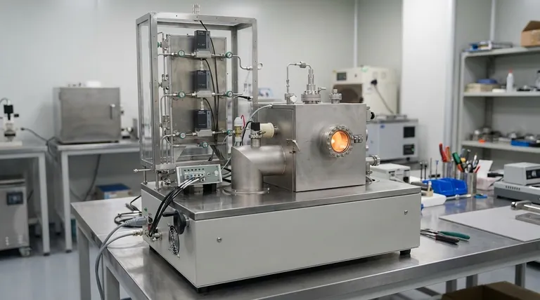
At its core, Chemical Vapor Deposition (CVD) is a sophisticated process that transforms gases into a solid, high-performance thin film on a substrate. It involves introducing reactive precursor gases into a chamber where they decompose and react on a heated surface, building the desired material one atomic layer at a time. The fundamental steps include the transport of these gases to the substrate, their chemical reaction on the surface to form a solid, and the removal of the gaseous byproducts.
The crucial insight is that CVD is not merely a coating technique; it is a controlled chemical synthesis that occurs directly on a surface. Understanding the sequence of events—from gas delivery to surface reaction and byproduct removal—is key to controlling the final material's properties.
Deconstructing the CVD Process
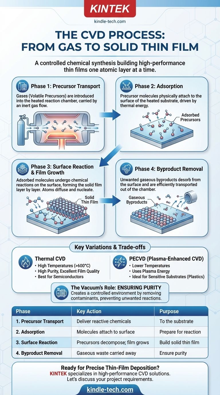
The entire process can be broken down into four distinct phases, each critical for achieving a high-quality, uniform film. This sequence represents the journey of a precursor molecule from a gas into a solid structure.
Phase 1: Precursor Introduction and Transport
The process begins with the delivery of reactive gases, known as precursors, into a reaction chamber.
These precursors are volatile compounds containing the elements you want to deposit. They are transported towards the target substrate, typically carried by an inert gas flow.
Phase 2: Adsorption onto the Substrate
Once the precursor gases reach the substrate, they physically attach to its surface in a process called adsorption.
The substrate itself is heated to a specific temperature, providing the necessary thermal energy to drive the upcoming reactions. This stage is simply about getting the reactive molecules to "land and stick" on the surface.
Phase 3: The Surface Reaction and Film Growth
This is the heart of the CVD process, where the chemical transformation occurs. The adsorbed precursor molecules absorb energy from the heated surface and undergo chemical reactions.
These reactions break the precursors down, allowing the desired atoms to bond with the substrate surface. The atoms then diffuse (move across the surface) to find energetically favorable locations, forming stable crystal structures in a step called nucleation. This process repeats, growing the thin film layer by layer.
Phase 4: Desorption and Removal of Byproducts
The chemical reactions that form the solid film also create unwanted gaseous byproducts.
These byproduct molecules must desorb (detach) from the substrate surface and be transported out of the reaction chamber by the gas flow. Efficient removal is critical to prevent these byproducts from contaminating the growing film.
Understanding Key Variations and Trade-offs
The "standard" process described above is known as Thermal CVD, but several variations exist to meet different needs. The primary trade-off is often between deposition temperature and film quality.
Thermal CVD vs. Plasma-Enhanced CVD (PECVD)
Thermal CVD relies solely on high temperatures (often >600°C) to provide the energy for the chemical reaction. This produces very pure, high-quality films but can damage temperature-sensitive substrates like plastics or certain electronics.
Plasma-Enhanced CVD (PECVD) uses an electric field to generate a plasma (an ionized gas). This highly energetic plasma can break down precursor gases at much lower temperatures, making it ideal for deposition on sensitive materials.
The Critical Role of the Vacuum
A common misconception is that the vacuum "pulls" chemicals onto the workpiece. In reality, the vacuum's primary purpose is to ensure purity.
By removing air and other contaminants from the chamber, you create a controlled environment where only the intended precursor gases can react. This prevents the formation of unwanted oxides or nitrides in the final film.
Applying This to Your Project
The right CVD method depends entirely on the material you are depositing and the substrate you are using.
- If your primary focus is on high-purity, crystalline films (e.g., for semiconductors): Thermal CVD is often the superior choice due to the excellent film quality achieved at high temperatures.
- If your primary focus is depositing on temperature-sensitive materials (e.g., polymers or assembled electronics): PECVD is the necessary approach, as it allows for quality film growth at significantly lower temperatures.
- If your primary focus is growing complex, multi-element films (e.g., advanced semiconductors or LEDs): A specialized technique like Metalorganic CVD (MOCVD) is used, which offers precise control over the composition.
Ultimately, mastering CVD is about precisely controlling this sequence of chemical events to build materials from the atom up.
Summary Table:
| Phase | Key Action | Purpose |
|---|---|---|
| 1. Precursor Transport | Gases are introduced into the chamber | Deliver reactive chemicals to the substrate |
| 2. Adsorption | Molecules attach to the heated surface | Prepare for the chemical reaction |
| 3. Surface Reaction | Precursors decompose; film grows layer by layer | Build the solid thin film |
| 4. Byproduct Removal | Gaseous waste is carried away | Ensure film purity and quality |
Ready to achieve precise thin-film deposition for your lab?
KINTEK specializes in high-performance lab equipment and consumables for advanced processes like CVD. Whether you need a robust Thermal CVD system for high-purity films or a versatile PECVD solution for temperature-sensitive substrates, our expertise ensures you get the right tool for your research or production needs.
Let's discuss your project requirements. Contact our experts today to find the perfect CVD solution for your laboratory.
Visual Guide
Related Products
- Chemical Vapor Deposition CVD Equipment System Chamber Slide PECVD Tube Furnace with Liquid Gasifier PECVD Machine
- RF PECVD System Radio Frequency Plasma-Enhanced Chemical Vapor Deposition RF PECVD
- Microwave Plasma Chemical Vapor Deposition MPCVD Machine System Reactor for Lab and Diamond Growth
- Customer Made Versatile CVD Tube Furnace Chemical Vapor Deposition Chamber System Equipment
- 915MHz MPCVD Diamond Machine Microwave Plasma Chemical Vapor Deposition System Reactor
People Also Ask
- Why is Chemical Vapor Deposition (CVD) equipment uniquely suited for constructing hierarchical superhydrophobic structures?
- What are the core advantages of PE-CVD in OLED encapsulation? Protect Sensitive Layers with Low-Temp Film Deposition
- What are the processes of vapor phase deposition? Understand CVD vs. PVD for Superior Thin Films
- How expensive is chemical vapor deposition? Understanding the True Cost of High-Performance Coating
- How are carbon nanotubes grown? Master Scalable Production with Chemical Vapor Deposition


