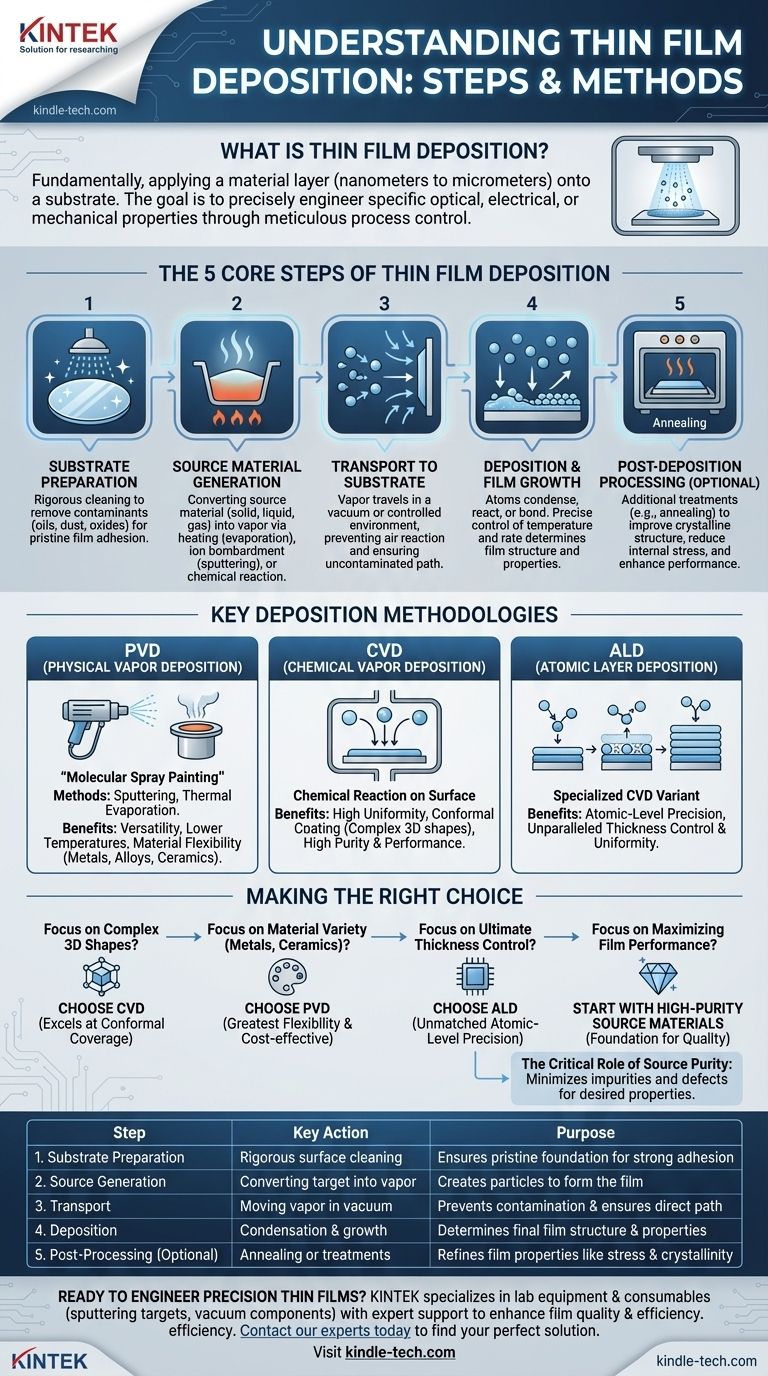
Fundamentally, thin film deposition is a process of applying a material layer, ranging from a few nanometers to several micrometers thick, onto a surface or substrate. This process consists of five core stages: preparing the substrate, generating a vapor from a source material, transporting this vapor to the substrate within a vacuum or controlled environment, depositing it to form a solid film, and optionally treating the film to refine its properties.
The goal of thin film deposition is not merely to coat a surface, but to precisely engineer a film with specific optical, electrical, or mechanical properties by meticulously controlling each step of the deposition process.
The Universal Steps of Thin Film Deposition
Regardless of the specific technology used, every deposition process follows a similar fundamental sequence. Understanding these stages is key to controlling the final quality of the film.
Step 1: Substrate Preparation
Before deposition can begin, the substrate must be rigorously cleaned and prepared. Any surface contaminants, such as oils, dust, or oxides, will create defects and prevent the film from adhering properly. This stage ensures a pristine foundation for film growth.
Step 2: Source Material Generation
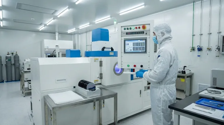
A source material, often called a target, is selected based on the desired film composition. This material, which can be a solid, liquid, or gas, is then converted into a vaporous state. This is accomplished using energy from methods like heating (evaporation), ion bombardment (sputtering), or chemical reaction.
Step 3: Transport to the Substrate
The generated vapor of atoms or molecules must travel from the source to the substrate. This almost always occurs within a vacuum chamber to prevent the vapor from reacting with air and to ensure a direct, uncontaminated path to the substrate surface.
Step 4: Deposition and Film Growth
Upon reaching the substrate, the vapor condenses, reacts, or bonds with the surface. Atoms nucleate at various points and coalesce to form a continuous layer. The precise control of parameters like substrate temperature and deposition rate determines the film's structure and properties.
Step 5: Post-Deposition Processing (Optional)
After the film is formed, it may undergo additional treatments. Annealing, a process of heating the film in a controlled environment, can be used to improve its crystalline structure, reduce internal stress, and enhance its overall performance.
Key Deposition Methodologies
While the steps are universal, the methods for executing them vary significantly. The choice of method depends on the material being deposited and the required film characteristics.
Physical Vapor Deposition (PVD)
PVD is a process where a material is physically removed from a solid source and deposited onto the substrate. Think of it as a form of "molecular spray painting."
Common PVD techniques include sputtering, which uses an ion beam to dislodge atoms from a target, and thermal evaporation, which heats the material until it vaporizes.
Chemical Vapor Deposition (CVD)
CVD builds a film through a chemical reaction on the substrate's surface. Precursor gases are introduced into a reaction chamber, and when they come into contact with the heated substrate, they react and decompose, leaving behind a solid film.
This method is prized in the semiconductor industry for its ability to produce highly uniform (conformal) coatings over complex surfaces.
Atomic Layer Deposition (ALD)
ALD is a highly specialized variant of CVD that deposits a film one single atomic layer at a time. It uses a sequence of self-limiting chemical reactions, providing unparalleled precision in controlling film thickness and uniformity.
Understanding the Trade-offs
Choosing the right deposition method is a critical decision driven by the specific requirements of the application. No single method is universally superior.
PVD: Versatility and Lower Temperatures
PVD is highly versatile and can be used to deposit a vast range of materials, including metals, alloys, and ceramics. Because it is often a lower-temperature process compared to CVD, it is suitable for coating substrates that are sensitive to heat.
CVD: Conformality and Purity
CVD excels at creating exceptionally uniform films that can conformally coat intricate 3D structures. This makes it essential for many microelectronics applications. It is often the method of choice for producing very high-purity, high-performance films.
The Critical Role of Source Purity
Regardless of the method, the quality of the final film is directly tied to the purity of the source material. Using high-purity sputtering targets or precursor gases minimizes impurities and defects, which is essential for achieving the desired electrical, optical, or mechanical properties.
Making the Right Choice for Your Goal
Your application's primary goal will dictate the most appropriate deposition strategy.
- If your primary focus is coating a complex 3D shape uniformly: Your best choice is likely CVD, which excels at conformal coverage.
- If your primary focus is depositing a wide variety of metals or ceramics: PVD offers the greatest material flexibility and is often more cost-effective for these applications.
- If your primary focus is achieving ultimate control over film thickness for advanced electronics: ALD provides atomic-level precision that is unmatched by other methods.
- If your primary focus is maximizing film performance and reliability: Begin by investing in the highest-purity source materials available, as this is the foundation for quality.
By mastering these fundamental steps and methods, you move from simply applying a coating to precisely engineering material properties at the atomic scale.
Summary Table:
| Step | Key Action | Purpose |
|---|---|---|
| 1. Substrate Preparation | Rigorous cleaning of the surface | Ensures a pristine foundation for strong film adhesion |
| 2. Source Generation | Converting target material into a vapor | Creates the particles that will form the film |
| 3. Transport | Moving vapor to substrate in a vacuum | Prevents contamination and ensures a direct path |
| 4. Deposition | Condensation and growth of the film layer | Determines the film's final structure and properties |
| 5. Post-Processing (Optional) | Annealing or other treatments | Refines film properties like stress and crystallinity |
Ready to engineer thin films with precision? The right equipment and high-purity materials are fundamental to your success. KINTEK specializes in lab equipment and consumables, providing reliable sputtering targets, vacuum components, and expert support for your deposition needs. Let's discuss how our solutions can enhance your film quality and process efficiency.
Contact our experts today to find the perfect deposition solution for your laboratory.
Visual Guide
Related Products
- Aluminized Ceramic Evaporation Boat for Thin Film Deposition
- Tungsten Evaporation Boat for Thin Film Deposition
- Electron Beam Evaporation Coating Oxygen-Free Copper Crucible and Evaporation Boat
- Molybdenum Tungsten Tantalum Evaporation Boat for High Temperature Applications
- HFCVD Machine System Equipment for Drawing Die Nano-Diamond Coating
People Also Ask
- Why are high-purity ceramic boats used for lignin activation? Ensure Purity & Thermal Stability
- What is the chemical method for thin film deposition? Build Films from the Molecular Level Up
- What are the alternatives to sputtering? Choose the Right Thin Film Deposition Method
- What is the source of evaporation for thin film? Choosing Between Thermal and E-Beam Methods
- What is thin film deposition? Unlock Advanced Surface Engineering for Your Materials


