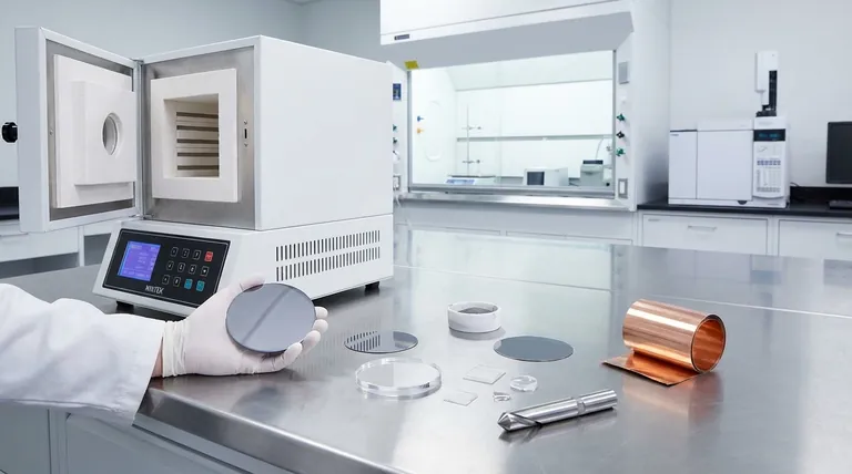
In Chemical Vapor Deposition (CVD), the term "substrate" refers to the material or workpiece onto which a thin film is grown. While an extremely wide variety of materials can be deposited, the choice of substrate is primarily governed by its ability to withstand the high temperatures of the CVD process and its compatibility with the desired film. Common examples include silicon wafers for electronics, tool steels and cemented carbides for hard coatings, and quartz or sapphire for optical applications.
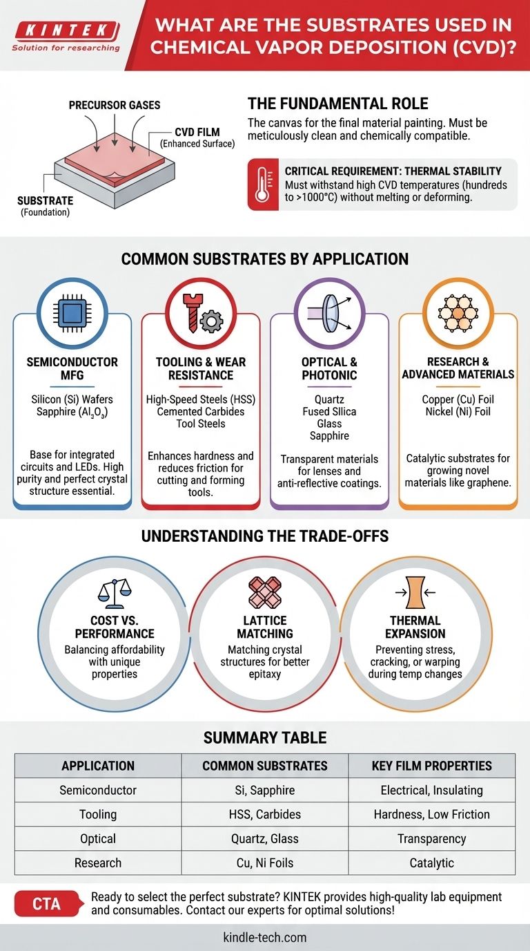
The most critical requirement for a CVD substrate is not its material type, but its thermal stability. The substrate must remain physically and chemically intact at the specific reaction temperatures required to deposit the desired film, which often range from several hundred to over a thousand degrees Celsius.
The Fundamental Role of the Substrate
In any CVD process, the substrate acts as the foundation. It is the surface where precursor gases react to form the solid thin film. Think of it as the canvas upon which the final material "painting" is created.
Thermal Stability is Non-Negotiable
CVD relies on thermally-driven chemical reactions. If a substrate melts, deforms, or outgasses at the deposition temperature, the process will fail. This single requirement immediately rules out most plastics and low-melting-point metals for conventional, high-temperature CVD.
Surface and Chemical Compatibility
The substrate surface must be meticulously clean to ensure the film adheres properly and grows uniformly. Furthermore, the substrate material should not react undesirably with the precursor gases in a way that contaminates the film or damages the substrate itself.
Common Substrates by Application
The choice of substrate is entirely dependent on the final application of the coated part. The substrate provides the core function (e.g., the shape of a cutting tool, the semiconducting property of a wafer), while the CVD film enhances its surface properties.
For Semiconductor Manufacturing
The dominant substrate is the silicon (Si) wafer. It serves as the base for depositing layers of polysilicon, silicon nitride (Si₃N₄), and various metals that form integrated circuits. Its high purity and perfect crystal structure are essential. For specialized devices like high-brightness LEDs, sapphire (Al₂O₃) is also a common substrate.
For Tooling and Wear Resistance
To enhance hardness and reduce friction, CVD coatings are applied to materials used in cutting, forming, and molding. Key substrates include high-speed steels (HSS), cemented carbides (often called tungsten carbide), and various tool steels. These are coated with materials like titanium nitride (TiN) and titanium carbonitride (TiCN).
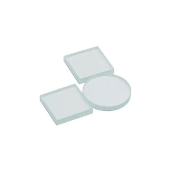
For Optical and Photonic Applications
When the final product must transmit light, the substrate must be transparent in the desired wavelength range. Common choices include quartz, fused silica, various types of glass, and sapphire. These are used as substrates for anti-reflective coatings or protective optical films.
For Research and Advanced Materials
In materials science, researchers often use specific substrates to catalyze the growth of novel materials. For example, copper (Cu) and nickel (Ni) foils are widely used as catalytic substrates for growing large-area sheets of graphene.
Understanding the Trade-offs
Selecting a substrate is a balancing act between ideal properties and practical constraints.
Cost vs. Performance
A standard silicon wafer offers incredible performance for its cost, enabling the entire microelectronics industry. In contrast, a large, single-crystal sapphire wafer is significantly more expensive and reserved for applications where its unique properties (like transparency and electrical insulation) are indispensable.
Lattice Matching and Crystal Growth
For high-performance electronics or optics, it is often desirable to grow a single-crystal film. This process, called epitaxy, works best when the crystal lattice of the substrate closely matches that of the film being grown. A mismatch can introduce defects and stress, degrading performance.
Thermal Expansion Mismatch
During heating and cooling, the substrate and the deposited film expand and contract. If their rates of thermal expansion are very different, immense stress can build up, leading to film cracking, peeling, or even warping of the substrate. This is a critical consideration for any CVD process.
Choosing the Right Substrate for Your Goal
The ideal substrate is dictated by your end goal. The film adds properties to the surface, but the substrate defines the object's fundamental purpose.
- If your primary focus is microelectronics: Your substrate will almost certainly be a single-crystal silicon wafer.
- If your primary focus is mechanical hardness: Your substrate will be a component made of tool steel or cemented carbide.
- If your primary focus is optical transparency: Your substrate will be a material like quartz, glass, or sapphire.
- If your primary focus is novel 2D material synthesis: You will likely use a catalytic metal substrate like copper or nickel foil.
Ultimately, the substrate is the critical foundation that determines the function, performance, and viability of the final product.
Summary Table:
| Application | Common Substrates | Key Film Properties |
|---|---|---|
| Semiconductor Manufacturing | Silicon (Si) wafers, Sapphire (Al₂O₃) | Electrical, Insulating |
| Tooling & Wear Resistance | High-Speed Steels (HSS), Cemented Carbides | Hardness, Low Friction |
| Optical & Photonic Devices | Quartz, Glass, Fused Silica | Transparency, Anti-Reflection |
| Advanced Materials Research | Copper (Cu) foil, Nickel (Ni) foil | Catalytic (e.g., for Graphene) |
Ready to select the perfect substrate for your CVD application? KINTEK specializes in providing high-quality lab equipment and consumables for all your laboratory needs. Our experts can help you choose the right materials to ensure optimal film adhesion, thermal stability, and performance for your specific project. Contact us today to discuss your requirements and discover how KINTEK's solutions can enhance your research and production processes!
Visual Guide
Related Products
- Optical Window Glass Substrate Wafer Quartz Plate JGS1 JGS2 JGS3
- MgF2 Magnesium Fluoride Crystal Substrate Window for Optical Applications
- Conductive Carbon Cloth Carbon Paper Carbon Felt for Electrodes and Batteries
- Customer Made Versatile CVD Tube Furnace Chemical Vapor Deposition Chamber System Equipment
- Custom CVD Diamond Coating for Lab Applications
People Also Ask
- What is the maximum temperature for quartz windows? Ensure Long-Term Reliability and Avoid Devitrification
- What is the temperature range of quartz glass? Master Its Thermal Limits for Demanding Applications
- What is the working temperature of quartz glass? Master Its High-Temp Limits & Applications
- What are the uses of quartz glass? Essential for Extreme-Temperature and UV Applications
- What is optical quartz? The Ultimate Material for UV and High-Temp Optics