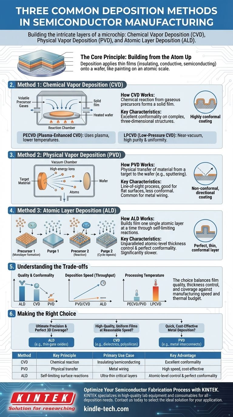
At its core, semiconductor manufacturing relies on three principal deposition methods to build the intricate layers of a microchip: Chemical Vapor Deposition (CVD), Physical Vapor Deposition (PVD), and Atomic Layer Deposition (ALD). CVD uses chemical reactions from gaseous precursors to form a solid film, PVD physically transfers material from a source to the wafer, and ALD builds films one single atomic layer at a time for ultimate precision.
The choice between these methods is never arbitrary. It is a fundamental engineering decision that balances the need for film quality, thickness control, and coverage against the practical constraints of manufacturing speed and thermal budget. Understanding this balance is key to understanding modern chip fabrication.
The Core Principle: Building from the Atom Up
Deposition is the process of applying thin films of various materials onto a semiconductor wafer. Think of it as painting, but on an atomic scale, where each layer serves a specific purpose in the chip's final electronic circuit.
These layers can be insulating (like silicon dioxide), conductive (like copper or aluminum), or semiconducting (like doped silicon). The method used to deposit each layer is chosen based on the material's properties and its role in the device's architecture.
Method 1: Chemical Vapor Deposition (CVD)
CVD is a versatile and widely used technique for creating high-quality, uniform films. It is the workhorse for depositing many of the insulating and semiconducting layers in a chip.
How CVD Works
In a CVD process, a wafer is placed in a reaction chamber and heated. Volatile precursor gases are then introduced, which contain the atoms needed for the final film. These gases react or decompose on the hot wafer surface, leaving behind a solid thin film.
Key Characteristics
The primary advantage of CVD is its ability to create highly conformal films. This means it can coat complex, three-dimensional structures uniformly, which is essential as transistors shrink and become more intricate.
Common Variations: PECVD & LPCVD
The broad CVD category includes several specialized techniques:
- Plasma-Enhanced CVD (PECVD): This method uses an energy-rich plasma to drive the chemical reactions. This allows deposition to occur at much lower temperatures, which is critical for preventing damage to previously fabricated components on the wafer.
- Low-Pressure CVD (LPCVD): By operating in a near-vacuum, LPCVD reduces unwanted gas-phase reactions. This results in films with very high purity and excellent uniformity across the entire wafer.
Method 2: Physical Vapor Deposition (PVD)
PVD, also known as sputtering, is fundamentally different from CVD. Instead of a chemical reaction, it uses a physical process to transfer material.
How PVD Works
A solid "target" made of the desired deposition material (e.g., a metal like aluminum or titanium) is placed in a vacuum chamber. High-energy ions, typically from an inert gas like argon, are fired at this target. The bombardment physically knocks atoms loose from the target, which then travel and coat the wafer.
Key Characteristics
PVD is a line-of-sight process. The sputtered atoms travel in a relatively straight line, much like paint from a spray can. This makes it excellent for depositing films on flat surfaces but poor at coating the sidewalls of deep trenches or complex topographies. It is most commonly used for depositing metal layers for wiring.
Method 3: Atomic Layer Deposition (ALD)
ALD is the most advanced deposition technique, offering unparalleled control over film thickness and conformality. It can be considered a highly precise sub-type of CVD.
How ALD Works
ALD builds a film one single atomic layer at a time through a sequence of self-limiting reactions.
- A precursor gas is introduced, reacting with the wafer surface to form a single, uniform monolayer. No further reaction can occur.
- The chamber is purged to remove any excess precursor gas.
- A second reactant gas is introduced, reacting only with the monolayer from step one to complete one layer of the final film.
- The chamber is purged again, and the cycle is repeated until the desired thickness is achieved.
Key Characteristics
The result is a perfectly conformal film with atomic-level thickness control. While this precision is unmatched, the process is significantly slower than CVD or PVD, making it suitable for only the most critical, ultra-thin layers in advanced transistors.
Understanding the Trade-offs
The choice of deposition method involves a critical evaluation of competing priorities. No single method is best for all applications.
Quality and Conformality
ALD provides the highest possible quality and perfect conformality, essential for wrapping around the 3D gates of modern transistors. CVD offers very good conformality and quality, suitable for most insulating and semiconducting layers. PVD has the lowest conformality due to its line-of-sight nature.
Deposition Speed (Throughput)
PVD and CVD are relatively fast processes, making them suitable for depositing the thicker films required in manufacturing, where throughput is critical. ALD is extremely slow by comparison, as it builds the film one atomic layer at a time.
Processing Temperature
The heat required for deposition can affect or damage existing structures on the chip. PECVD and PVD are valuable low-temperature options. Other methods, like LPCVD, often require higher temperatures to achieve the desired film properties, limiting when they can be used in the manufacturing flow.
Making the Right Choice for Your Goal
Selecting a deposition method requires aligning the technique's strengths with the specific architectural requirement of the film layer being built.
- If your primary focus is ultimate precision and perfect coverage on complex 3D structures: ALD is the necessary choice for the most critical, thin-gate oxides and high-k dielectrics, despite its slow speed.
- If your primary focus is high-quality, uniform films at a reasonable speed: CVD and its variants (like PECVD for lower temperatures) are the workhorses of the industry for most dielectric and polysilicon layers.
- If your primary focus is depositing metals quickly and cost-effectively: PVD (specifically sputtering) is the go-to method for creating the metal interconnects that wire the chip together.
Ultimately, a modern semiconductor is a complex sandwich of dozens of layers, each deposited with the specific tool best suited for the job.
Summary Table:
| Method | Full Name | Key Principle | Primary Use Case | Key Advantage |
|---|---|---|---|---|
| CVD | Chemical Vapor Deposition | Chemical reaction from gases | Insulating & semiconducting layers | Excellent conformality on complex structures |
| PVD | Physical Vapor Deposition | Physical transfer of material (sputtering) | Metal wiring layers | High speed, cost-effective for metals |
| ALD | Atomic Layer Deposition | Self-limiting surface reactions | Ultra-thin, critical layers (e.g., gate oxides) | Atomic-level thickness control & perfect conformality |
Optimize Your Semiconductor Fabrication Process with KINTEK
Choosing the right deposition method is critical to the performance and yield of your semiconductor devices. Whether your priority is the ultimate precision of ALD, the versatile conformality of CVD, or the high-speed metal deposition of PVD, having the right equipment is paramount.
KINTEK specializes in providing high-quality lab equipment and consumables for all your deposition needs. Our expertise can help you navigate these critical trade-offs to select the ideal solution for your specific application, ensuring superior film quality and manufacturing efficiency.
Contact us today to discuss how our solutions can enhance your lab's capabilities and drive your next innovation forward.
Get in touch with our experts now!
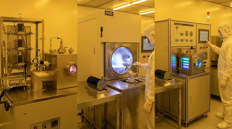
Visual Guide
Related Products
- Customer Made Versatile CVD Tube Furnace Chemical Vapor Deposition Chamber System Equipment
- CVD Diamond Dressing Tools for Precision Applications
- Chemical Vapor Deposition CVD Equipment System Chamber Slide PECVD Tube Furnace with Liquid Gasifier PECVD Machine
- Multi Heating Zones CVD Tube Furnace Machine Chemical Vapor Deposition Chamber System Equipment
- CVD Diamond for Thermal Management Applications
People Also Ask
- What is a CVD furnace? The Ultimate Guide to Precision Thin-Film Coating
- What is the effect of temperature on graphene oxide? Master Thermal Reduction for Precise Material Properties
- What is chemical vapor deposition for CNT? The Leading Method for Scalable Carbon Nanotube Synthesis
- What is a CVD tube furnace? A Complete Guide to Thin-Film Deposition
- What is the function of a high-temperature CVD tube furnace in 3D graphene foam prep? Master 3D Nanomaterial Growth


