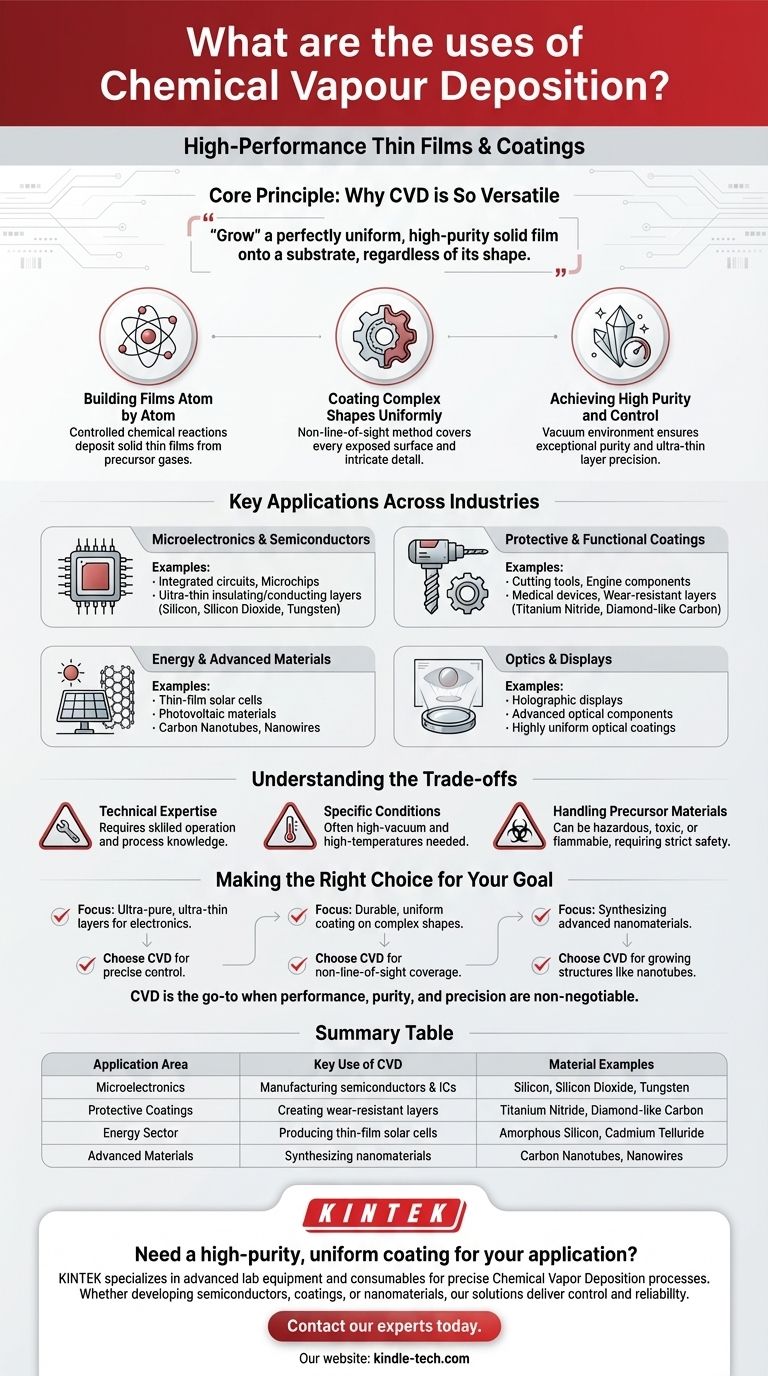
In short, Chemical Vapor Deposition (CVD) is used to create high-performance thin films and coatings for a vast range of applications. Its primary uses are in the electronics industry for manufacturing semiconductors, in heavy industry for creating durable and corrosion-resistant coatings on cutting tools, and in the energy sector for producing thin-film solar cells.
The core reason CVD is so widely adopted is its unique ability to use gas-phase chemical reactions to "grow" a perfectly uniform, high-purity solid film onto a substrate, regardless of its shape. This gives engineers precise control over the material's thickness and properties.
The Core Principle: Why CVD is So Versatile
Chemical Vapor Deposition is not simply a coating method; it is a material synthesis process. Understanding its fundamental advantages explains its broad utility across different industries.
Building Films Atom by Atom
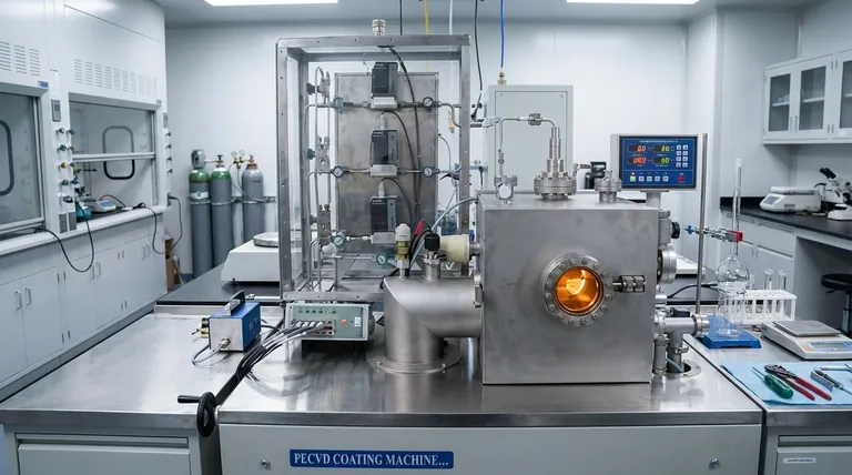
The process involves introducing precursor gases into a vacuum chamber containing the object to be coated (the substrate). These gases react or decompose on the substrate's hot surface, depositing a solid thin film.
This reliance on controlled chemical reactions is what gives CVD its power. By changing the gases, temperature, and pressure, you can deposit a wide variety of materials, including metals, ceramics, and semiconductors.
Coating Complex Shapes Uniformly
Unlike spray-on or line-of-sight methods, CVD uses gases that flow and diffuse to cover every exposed surface of an object. This is a critical non-line-of-sight advantage.
This ensures that even components with complex geometries, internal channels, or intricate patterns receive a completely uniform and even coating.
Achieving High Purity and Control
Because the process occurs in a controlled vacuum environment with highly refined precursor gases, the resulting films are exceptionally pure.
Furthermore, engineers have full control over the timing and rate of the deposition process. This allows for the creation of ultra-thin layers of material with precision, a capability essential for modern electronics.
Key Applications Across Industries
The unique advantages of CVD make it a foundational technology in several high-tech fields.
In Microelectronics and Semiconductors
This is arguably the most significant application of CVD. It is used to deposit the various thin films that make up integrated circuits and microchips.
The ability to create flawless, ultra-thin insulating or conducting layers is fundamental to building modern electronic devices.
For Protective and Functional Coatings
CVD is used to apply extremely hard and durable coatings to industrial cutting tools, drills, and engine components. These ceramic coatings prevent corrosion and dramatically reduce wear, extending the life of the tool.
This same principle is used for medical devices, automotive parts, and any application where surface durability is critical.
In Energy and Advanced Materials
The technology is used to deposit photovoltaic materials onto substrates to create thin-film solar cells.
CVD is also a primary method for growing advanced materials from the ground up, such as high-purity carbon nanotubes and various nanowires for next-generation electronics and composites.
For Optics and Displays
The process can create highly uniform and precise optical coatings. This is leveraged in specialized applications, including the manufacturing of holographic displays and other advanced optical components.
Understanding the Trade-offs
While powerful, CVD is not a universal solution. It comes with specific requirements and complexities that make it suitable for high-value applications.
Requires Technical Expertise
Operating CVD equipment is not a simple task. It demands a high level of skill and process knowledge to manage the vacuum, gas flows, and temperature profiles required to achieve a successful deposition.
The Need for Specific Conditions
Most CVD processes require a high-vacuum environment and often very high temperatures to initiate the necessary chemical reactions on the substrate's surface. This adds to the equipment's complexity and energy cost.
Handling of Precursor Materials
The precursor gases used in CVD can be hazardous, toxic, or flammable. Safely handling, storing, and disposing of these materials requires significant infrastructure and strict safety protocols.
Making the Right Choice for Your Goal
Deciding if CVD is the appropriate process depends entirely on the required outcome for the material's surface.
- If your primary focus is creating ultra-pure, ultra-thin layers for electronics: CVD is a foundational technology due to its precise control over film thickness and purity.
- If your primary focus is applying a durable, uniform coating to a complex shape: CVD is an excellent choice because its non-line-of-sight nature ensures even coverage on intricate surfaces.
- If your primary focus is synthesizing advanced nanomaterials: CVD is a standard and effective method for growing structures like carbon nanotubes and nanowires.
Ultimately, Chemical Vapor Deposition is the go-to process when performance, purity, and precision at the microscopic level are non-negotiable.
Summary Table:
| Application Area | Key Use of CVD | Material Examples |
|---|---|---|
| Microelectronics | Manufacturing semiconductors & integrated circuits | Silicon, Silicon Dioxide, Tungsten |
| Protective Coatings | Creating wear-resistant layers on tools & components | Titanium Nitride, Diamond-like Carbon |
| Energy Sector | Producing thin-film solar cells | Amorphous Silicon, Cadmium Telluride |
| Advanced Materials | Synthesizing nanomaterials like carbon nanotubes | Carbon Nanotubes, Nanowires |
Need a high-purity, uniform coating for your application?
KINTEK specializes in providing advanced lab equipment and consumables for precise Chemical Vapor Deposition processes. Whether you are developing next-generation semiconductors, durable protective coatings, or advanced nanomaterials, our solutions deliver the control and reliability your laboratory requires.
Contact our experts today to discuss how we can support your specific project goals and enhance your research and development capabilities.
Visual Guide
Related Products
- CVD Diamond Dressing Tools for Precision Applications
- Multi Heating Zones CVD Tube Furnace Machine Chemical Vapor Deposition Chamber System Equipment
- CVD Diamond Domes for Industrial and Scientific Applications
- CVD Diamond for Thermal Management Applications
- Chemical Vapor Deposition CVD Equipment System Chamber Slide PECVD Tube Furnace with Liquid Gasifier PECVD Machine
People Also Ask
- What color diamonds are CVD? Understanding the Process from Brown Tint to Colorless Beauty
- Does the chemical vapor deposition be used for diamonds? Yes, for Growing High-Purity Lab Diamonds
- What is chemical vapor deposition of diamond? Grow High-Purity Diamonds Atom-by-Atom
- What are the raw materials for CVD diamonds? A seed, a gas, and the science of crystal growth.
- Can CVD diamonds change color? No, their color is permanent and stable.


