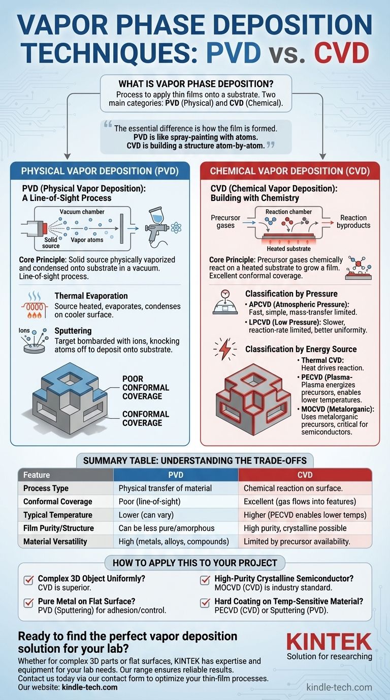
At its core, vapor phase deposition is a family of processes used to apply extremely thin films of material onto a surface, known as a substrate. The two fundamental categories are Physical Vapor Deposition (PVD), where a material is physically vaporized and transferred, and Chemical Vapor Deposition (CVD), where precursor gases react on the substrate's surface to grow a new material layer.
The essential difference is how the film is formed. PVD is a physical process, like spray-painting with atoms. CVD is a chemical process, like building a structure atom-by-atom through controlled reactions.
Physical Vapor Deposition (PVD): A Line-of-Sight Process
PVD techniques operate within a vacuum and involve physically transforming a solid source material into a vapor, which then condenses onto the substrate. This is a line-of-sight process, meaning atoms travel in a straight line from the source to the substrate.
The Core Principle of PVD
A target material is bombarded with energy, causing atoms or molecules to be ejected. These particles travel through a vacuum chamber and deposit onto the substrate, forming a thin film.
Thermal Evaporation
This is one of the simplest PVD methods. A source material is heated in a high vacuum until it evaporates or sublimes. The resulting vapor then travels and condenses on a cooler substrate, much like steam condensing on a cold mirror.
Sputtering
In sputtering, a target of the desired material is bombarded with high-energy ions (typically from an inert gas like Argon) in a plasma. This bombardment acts like a microscopic shotgun, physically knocking atoms off the target. These ejected atoms then deposit onto the substrate, creating a dense and strongly adhered film.
Chemical Vapor Deposition (CVD): Building with Chemistry
CVD is a fundamentally different approach. Instead of physically transferring a solid material, it introduces one or more volatile precursor gases into a reaction chamber. These gases decompose or react on a heated substrate to form the desired solid film.
The Core Principle of CVD
The essence of CVD is a chemical reaction on a surface. Because it relies on gases that can flow around and into features, CVD offers excellent conformal coverage, meaning it can coat complex, three-dimensional shapes uniformly.
Classification by Pressure
The chamber pressure dramatically affects the deposition process.
- Atmospheric Pressure CVD (APCVD): Performed at normal atmospheric pressure. It is fast and simple but often limited by how quickly precursor gases can get to the surface (mass-transfer limited), which can affect film uniformity.
- Low Pressure CVD (LPCVD): Performed at reduced pressures. This slows the process but allows gases to diffuse more evenly, making the deposition reaction-rate limited. The result is superior uniformity and purity, which is critical for electronics.
Classification by Energy Source
Heat is the traditional way to drive the reaction, but other energy sources allow for more control and lower temperatures.
- Thermal CVD: The substrate is heated, providing the thermal energy needed for the precursors to react.
- Plasma-Enhanced CVD (PECVD): A plasma is used to energize the precursor gases, allowing deposition to occur at much lower temperatures than in thermal CVD. This is crucial for coating heat-sensitive substrates like plastics or certain electronic devices.
- Metalorganic CVD (MOCVD): This specialized technique uses metalorganic compounds as precursors and is a cornerstone of the modern semiconductor industry for manufacturing high-performance LEDs and transistors.
Understanding the Trade-offs: PVD vs. CVD
Choosing between PVD and CVD requires understanding their inherent strengths and weaknesses.
Conformal Coverage (Coating Complex Shapes)
CVD excels here. The gaseous precursors can flow into deep trenches and coat intricate surfaces uniformly. PVD is poor at this because it is a line-of-sight process, creating "shadows" behind raised features.
Deposition Temperature
Traditional CVD requires high temperatures to drive chemical reactions. However, techniques like PECVD allow for low-temperature deposition. PVD can often be performed at lower temperatures, though the substrate can still heat up significantly during the process.
Film Purity and Structure
CVD can produce exceptionally pure, crystalline films because the process is built from specific chemical reactions. PVD films are more prone to incorporating impurities from the chamber and can have a less-ordered, amorphous structure unless the process is carefully controlled.
Material Versatility
PVD is more versatile for pure metals, alloys, and compounds. Essentially, any material that can be physically vaporized or sputtered can be deposited. CVD is limited to materials for which suitable, stable, and often non-toxic precursor gases can be found.
How to Apply This to Your Project
Your choice depends entirely on the film's desired properties and the substrate you are using.
- If your primary focus is coating a complex 3D object uniformly: CVD is the superior choice due to its non-line-of-sight, gas-based deposition.
- If your primary focus is depositing a pure metal film on a flat surface: PVD, particularly sputtering, provides excellent adhesion and control.
- If your primary focus is growing a high-purity crystalline semiconductor layer: A specialized CVD process like MOCVD is the industry standard.
- If your primary focus is applying a hard coating to a temperature-sensitive material: PECVD (a type of CVD) or sputtering (a type of PVD) are both excellent low-temperature options.
Understanding the fundamental distinction between physical transfer (PVD) and chemical creation (CVD) empowers you to select the right tool for your specific engineering challenge.
Summary Table:
| Feature | PVD (Physical Vapor Deposition) | CVD (Chemical Vapor Deposition) |
|---|---|---|
| Process Type | Physical transfer of material | Chemical reaction on surface |
| Conformal Coverage | Poor (line-of-sight) | Excellent (gas flows into features) |
| Typical Temperature | Lower (can vary) | Higher (PECVD enables lower temps) |
| Film Purity/Structure | Can be less pure/amorphous | High purity, crystalline possible |
| Material Versatility | High (metals, alloys, compounds) | Limited by precursor availability |
Ready to find the perfect vapor deposition solution for your lab?
Whether you need the conformal coating of CVD for complex 3D parts or the precise metal deposition of PVD for flat surfaces, KINTEK has the expertise and equipment to meet your specific laboratory needs. Our range of high-quality lab equipment and consumables ensures you get reliable, high-performance results.
Contact us today via our contact form to discuss how we can help optimize your thin-film processes and enhance your research and development.
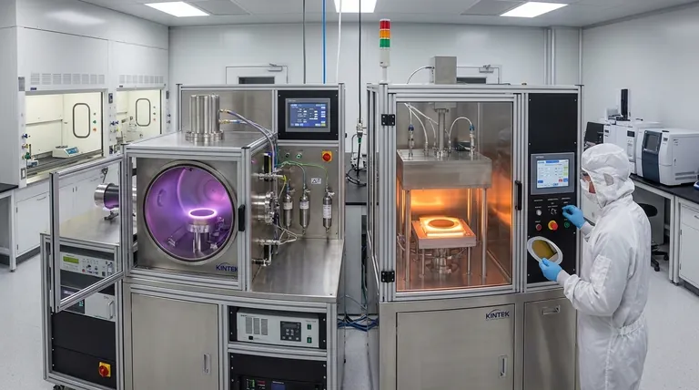
Visual Guide
Related Products
- Chemical Vapor Deposition CVD Equipment System Chamber Slide PECVD Tube Furnace with Liquid Gasifier PECVD Machine
- 915MHz MPCVD Diamond Machine Microwave Plasma Chemical Vapor Deposition System Reactor
- RF PECVD System Radio Frequency Plasma-Enhanced Chemical Vapor Deposition RF PECVD
- Microwave Plasma Chemical Vapor Deposition MPCVD Machine System Reactor for Lab and Diamond Growth
- HFCVD Machine System Equipment for Drawing Die Nano-Diamond Coating
People Also Ask
- What is the chemical vapor deposition growth process? Build Superior Thin Films from the Atom Up
- What is plasma enhanced chemical vapor deposition PECVD equipment? A Guide to Low-Temperature Thin Film Deposition
- How are carbon nanotubes grown? Master Scalable Production with Chemical Vapor Deposition
- Why is Chemical Vapor Deposition (CVD) equipment uniquely suited for constructing hierarchical superhydrophobic structures?
- What happens during deposition chemistry? Building Thin Films from Gaseous Precursors


