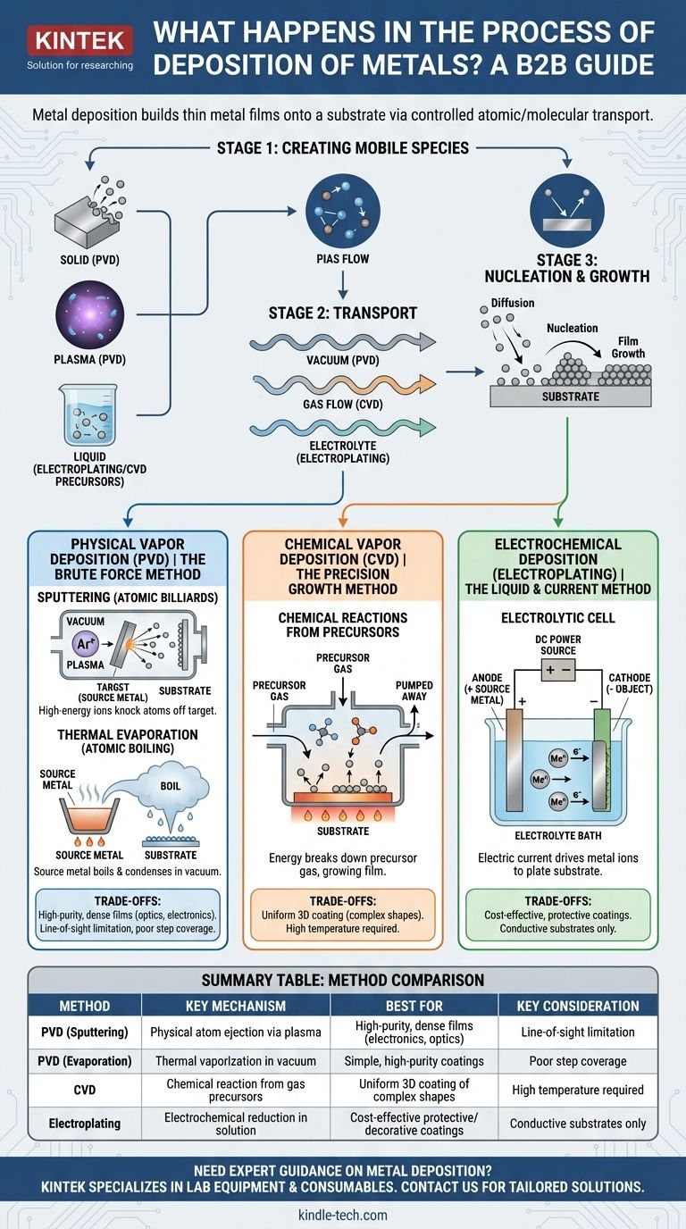
In short, metal deposition is any process that builds a thin film of metal onto a surface, known as a substrate. This is achieved by transporting metal atoms or ions from a source to the substrate, where they accumulate to form a solid layer. The specific method of transport and the state of the metal—whether it's a vapor, a plasma, or ions in a solution—define the different types of deposition.
The core principle of metal deposition is controlled atomic or molecular transport. Whether through physical force, chemical reaction, or electrical current, the goal is always the same: to move metal from a source to a substrate to build a new layer with specific, desired properties.
The Fundamental Process: From Source to Film
At its heart, all metal deposition involves three stages: creating mobile atoms/ions, transporting them to a surface, and getting them to stick and form a stable film. The "how" of these stages is what differentiates the major techniques.
Stage 1: Creating Mobile Metal Species
Before deposition can occur, metal atoms must be freed from their source material. This can be a solid block of metal, a chemical gas, or a liquid solution. The method used to liberate these atoms is a key defining factor of the overall process.
Stage 2: Transport to the Substrate
Once freed, the metal atoms or ions must travel to the target surface (the substrate). This journey can happen through a vacuum, within a flowing gas, or through a liquid electrolyte, often guided by electric or magnetic fields.
Stage 3: Nucleation and Growth
When atoms arrive at the substrate, they don't just instantly form a perfect layer. They land, move around on the surface (diffusion), and cluster together at energetic "sweet spots" to form stable islands, a process called nucleation. These islands then grow and merge to form a continuous film. The quality, grain structure, and stress of the final film are all determined during this critical stage.
Physical Vapor Deposition (PVD): The Brute Force Method
PVD encompasses methods that use physical processes like high-energy bombardment or heating to create a metal vapor, which then condenses on the substrate. This is typically done in a high-vacuum chamber to ensure purity.
Sputtering: Atomic Billiards
In sputtering, a chamber is filled with an inert gas, like argon, which is energized into a plasma. These high-energy gas ions are then accelerated into a solid metal "target." The impact is like a subatomic billiard break, knocking metal atoms off the target. These ejected atoms travel through the vacuum and coat the substrate.
Thermal Evaporation: Atomic Boiling
Evaporation is more intuitive. A source metal is heated in a vacuum chamber until it literally boils and evaporates, creating a cloud of metal vapor. This vapor travels in a straight line until it hits the cooler substrate, where it condenses back into a solid, forming a thin film.
Chemical Vapor Deposition (CVD): The Precision Growth Method
CVD uses chemical reactions to deposit films. Instead of physically knocking atoms off a target, it "grows" a film directly on the substrate from chemical precursors.
How It Works: Precursors and Reactions
In CVD, one or more volatile precursor gases containing the metal are introduced into a reaction chamber. Energy, usually in the form of heat, is applied to the substrate. This energy breaks down the precursor gases at the substrate's surface, freeing the metal atoms to bond to the surface while the other chemical byproducts are pumped away.
Electrochemical Deposition (Electroplating): The Liquid & Current Method
This common technique, also known as electroplating, uses a liquid solution and an electric current to deposit metal. It is fundamentally different from PVD and CVD because it does not occur in a vacuum or gas phase.
The Electrolytic Cell
The setup involves two electrodes submerged in an electrolyte bath containing dissolved metal ions. The object to be coated acts as the cathode (negative electrode), and a piece of the source metal often serves as the anode (positive electrode). When a direct current is applied, the metal ions in the solution are drawn to the cathode, where they gain electrons and are converted back into solid metal atoms, plating onto the object's surface.
Understanding the Trade-offs
No single deposition method is universally superior. The choice is a strategic trade-off based on the desired film properties, the substrate material, and cost.
Conformal Coverage (Uniformity)
CVD excels at coating complex, 3D shapes uniformly because the precursor gas can flow into and react within intricate features. PVD is a "line-of-sight" process, making it difficult to coat undercuts or the sides of deep trenches. Electroplating coverage depends on how evenly the electric current is distributed, which can be challenging on complex geometries.
Temperature and Substrate Limits
High-temperature CVD processes can damage sensitive substrates like plastics or certain electronic components. PVD methods, particularly sputtering, can often be performed at much lower temperatures, making them more versatile. Electroplating is a room-temperature, wet process, but it is only suitable for conductive substrates.
Film Purity and Density
PVD, especially sputtering, is known for producing very high-purity and dense films, which are critical for optical and semiconductor applications. CVD film purity is dependent on the purity of the precursor gases. Electroplating quality relies heavily on the cleanliness and composition of the electrolyte bath.
Making the Right Choice for Your Goal
Selecting a deposition technique requires aligning the process capabilities with the application's end goal.
- If your primary focus is high-purity, dense films for optics or electronics: PVD methods like sputtering are the industry standard for their control and quality.
- If your primary focus is uniformly coating a complex 3D part: CVD is the superior choice, provided your substrate can tolerate the processing temperatures.
- If your primary focus is a cost-effective protective or decorative coating on a conductive part: Electroplating offers excellent results with high throughput and relatively low cost.
Understanding these core mechanisms empowers you to select the precise tool needed to build functional materials, one atomic layer at a time.
Summary Table:
| Method | Key Mechanism | Best For | Key Consideration |
|---|---|---|---|
| PVD (Sputtering) | Physical atom ejection via plasma | High-purity, dense films (electronics, optics) | Line-of-sight limitation |
| PVD (Evaporation) | Thermal vaporization in vacuum | Simple, high-purity coatings | Poor step coverage |
| CVD | Chemical reaction from gas precursors | Uniform 3D coating of complex shapes | High temperature required |
| Electroplating | Electrochemical reduction in solution | Cost-effective protective/decorative coatings | Conductive substrates only |
Need expert guidance on metal deposition for your laboratory? KINTEK specializes in lab equipment and consumables for all your thin film coating needs. Whether you're working with PVD, CVD, or electroplating applications, our team can help you select the right equipment and materials to achieve precise, high-quality results. Contact our specialists today to discuss how we can support your research and production goals with tailored solutions for your specific substrate and coating requirements.
Visual Guide