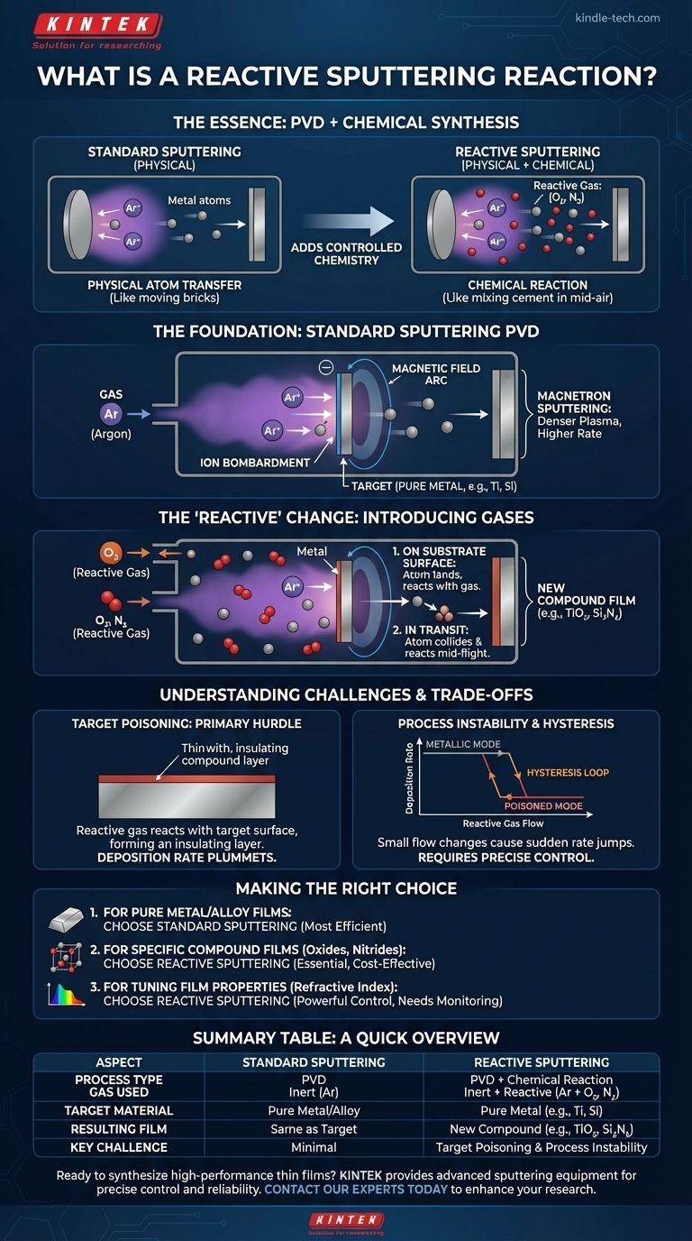
In essence, reactive sputtering is a thin-film deposition technique where a reactive gas is intentionally introduced into the vacuum chamber along with the standard inert gas. This process doesn't just physically deposit a material; it chemically synthesizes an entirely new compound film on the substrate's surface.
The crucial difference is this: standard sputtering physically transfers atoms from a source target to a substrate, like moving bricks from a pile. Reactive sputtering uses that same transfer process but adds a chemical reaction to create new materials, like mixing cement with sand in mid-air to form mortar as it lands.
The Foundation: Understanding Standard Sputtering
To grasp reactive sputtering, you must first understand the standard sputtering process it's built upon. It is a physical vapor deposition (PVD) method that occurs in a low-pressure vacuum environment.
The Core Mechanism: Ion Bombardment
The process begins by introducing an inert gas, almost always Argon (Ar), into the deposition chamber.
A high voltage is applied, creating a plasma of positively charged Argon ions (Ar+).
These high-energy ions are accelerated toward the source material, known as the target, which acts as the negative electrode (cathode). The ions collide with the target with enough force to knock out, or "sputter," individual atoms.
The Role of the Plasma and Inert Gas
The Argon gas doesn't chemically participate in the film formation. Its sole purpose is to be the "cannonball" that physically ejects material from the target.
This collision process creates a series of collision cascades on the target surface, dislodging atoms that then travel through the chamber and deposit onto the substrate, forming a thin film.
The Magnetron's Function
Modern systems use magnetron sputtering. Strong magnets are placed behind the target to create a magnetic field.
This field traps electrons near the target surface, significantly increasing the probability of them colliding with and ionizing the Argon gas atoms. This creates a denser, more stable plasma, leading to higher deposition rates.
The "Reactive" Element: How It Changes the Game
Reactive sputtering takes this physical process and adds a layer of controlled chemistry. The goal is to deposit a compound material (like an oxide or nitride) using a target that is often a pure, easy-to-sputter metal.
Introducing the Reactive Gas
The key step is bleeding a small, precisely controlled amount of a reactive gas, such as oxygen (O2) or nitrogen (N2), into the chamber along with the argon.
The sputtered atoms from the target are now traveling through a mix of inert and reactive gas molecules.
From Metal to Compound: Film Synthesis
As the sputtered metal atoms travel toward the substrate, they react with the gas. This chemical reaction can happen in two primary locations:
- On the substrate surface: The metal atom lands and then reacts with gas molecules that also land on the surface.
- In transit: The metal atom collides and reacts with a gas molecule mid-flight.
The result is the formation of a compound film. For example, by sputtering a pure titanium (Ti) target in an argon/oxygen mixture, you create a titanium dioxide (TiO2) film. Sputtering a silicon (Si) target in an argon/nitrogen mixture produces a silicon nitride (Si3N4) film.
Understanding the Trade-offs and Challenges
While powerful, reactive sputtering introduces complexities that require careful process control. It is not as straightforward as the purely physical process.
Target Poisoning: The Primary Hurdle
The most significant challenge is target poisoning. The reactive gas doesn't just react with the sputtered atoms; it also reacts with the surface of the target itself.
This forms a thin layer of the compound (e.g., an insulating oxide) on the conductive metal target. Because this compound layer sputters at a much lower rate than the pure metal, the deposition rate can plummet dramatically.
Process Instability and the Hysteresis Effect
This poisoning effect leads to process instability. There is a "hysteresis loop" where small changes in the reactive gas flow can cause a sudden, large jump between a high-rate metallic mode and a low-rate poisoned mode.
Navigating this instability is a core challenge in controlling the process to achieve repeatable, high-quality films.
Controlling Stoichiometry
Achieving the correct chemical composition, or stoichiometry, is critical. For instance, creating a perfectly transparent silicon dioxide (SiO2) film requires a very different gas balance than creating a sub-stoichiometric, absorptive SiOx film. This requires precise control over gas flow rates and power.
Making the Right Choice for Your Goal
Understanding the fundamentals allows you to select the right process for your specific material goal.
- If your primary focus is depositing a pure metal or a pre-made alloy: Standard non-reactive sputtering using only an inert gas is the correct and most efficient method.
- If your primary focus is creating a specific compound film (like an oxide, nitride, or carbide): Reactive sputtering is the essential and often most cost-effective technique, as it allows you to use a simple, robust metallic target.
- If your primary focus is tuning film properties (like refractive index or resistivity): Reactive sputtering offers powerful control by adjusting the gas mixture, but it demands sophisticated process monitoring to overcome instability.
Reactive sputtering transforms a simple physical deposition tool into a versatile platform for advanced materials synthesis.
Summary Table:
| Aspect | Standard Sputtering | Reactive Sputtering |
|---|---|---|
| Process Type | Physical Vapor Deposition (PVD) | PVD with Chemical Reaction |
| Gas Used | Inert Gas (e.g., Argon) | Inert Gas + Reactive Gas (e.g., O₂, N₂) |
| Target Material | Pure Metal or Alloy | Pure Metal (e.g., Ti, Si) |
| Resulting Film | Same as Target Material | New Compound (e.g., TiO₂, Si₃N₄) |
| Key Challenge | Minimal | Target Poisoning & Process Instability |
Ready to synthesize high-performance thin films like oxides and nitrides in your lab? KINTEK specializes in advanced sputtering equipment and consumables, providing the precise control and reliability needed to overcome challenges like target poisoning. Whether you're developing optical coatings, semiconductor layers, or protective films, our solutions are designed to enhance your research and production efficiency. Contact our experts today to discuss how we can support your specific laboratory needs!
Visual Guide
Related Products
- Spark Plasma Sintering Furnace SPS Furnace
- Chemical Vapor Deposition CVD Equipment System Chamber Slide PECVD Tube Furnace with Liquid Gasifier PECVD Machine
- RF PECVD System Radio Frequency Plasma-Enhanced Chemical Vapor Deposition RF PECVD
- Customer Made Versatile CVD Tube Furnace Chemical Vapor Deposition Chamber System Equipment
- Vacuum Induction Melting Spinning System Arc Melting Furnace
People Also Ask
- What is the difference between spark plasma sintering and flash sintering? A Guide to Advanced Sintering Methods
- What is the theory of spark plasma sintering? A Guide to Rapid, Low-Temperature Densification
- What are the fundamentals of spark plasma sintering process? Unlock Rapid, High-Performance Material Consolidation
- What are the advantages of CAMI/SPS for W-Cu composite preparation? Reduce cycles from hours to seconds.
- Why are Spark Plasma Sintering (SPS) furnaces or hot presses utilized in the preparation of Li3PS4 solid electrolytes?


