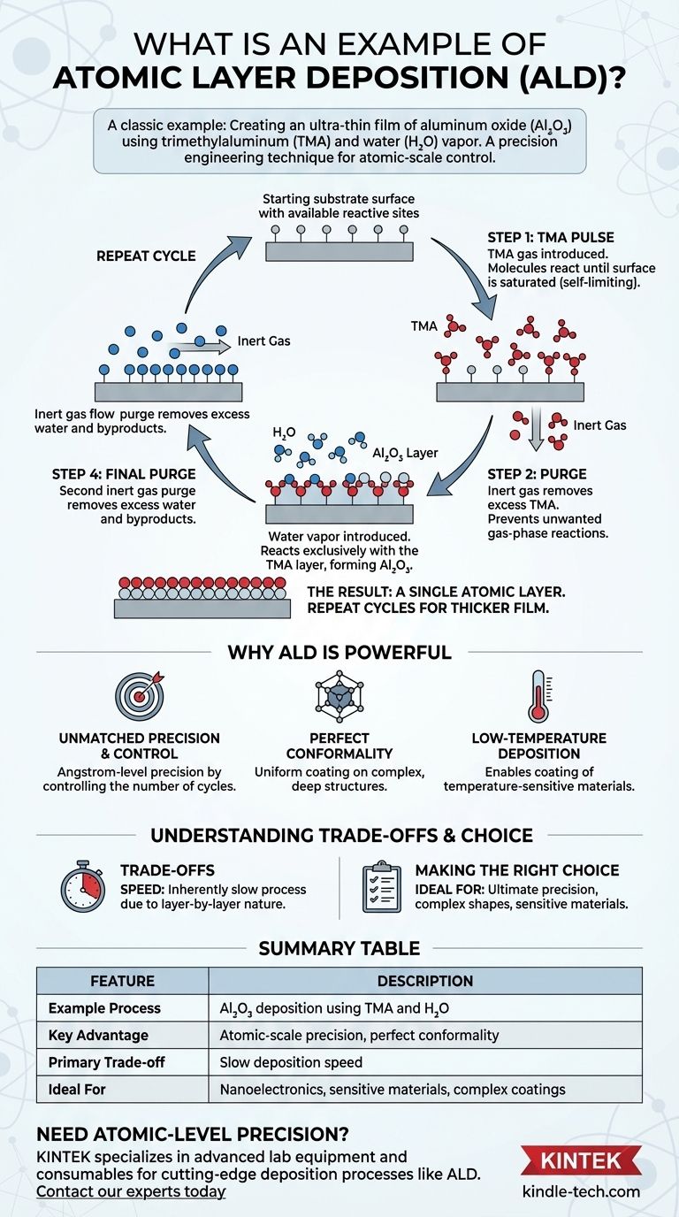
A classic example of atomic layer deposition (ALD) is the creation of an ultra-thin film of aluminum oxide (Al₂O₃) on a surface. This is achieved by sequentially exposing the surface to two chemical precursors: trimethylaluminum (TMA) and water (H₂O) vapor, with a purge step in between each exposure to remove excess reactants. The process builds a perfectly uniform film one atomic layer at a time.
Atomic layer deposition is not just a coating method; it's a precision engineering technique. Its power comes from using self-limiting chemical reactions to build materials with atomic-scale control, ensuring perfect uniformity even on the most complex three-dimensional structures.
How ALD Works: The Alumina Example in Detail
The deposition of aluminum oxide is a foundational example that clearly illustrates the cyclic, self-limiting nature of the ALD process. Each cycle deposits a single, predictable layer of material.
Step 1: The First Precursor (TMA)
Initially, a pulse of trimethylaluminum (TMA) gas is introduced into the reaction chamber. The TMA molecules react with the starting surface until every available reactive site is occupied. This reaction is self-limiting; once the surface is saturated, no more TMA can attach.
Step 2: The First Purge
An inert gas, like nitrogen or argon, is then flushed through the chamber. This purge completely removes any excess TMA molecules that did not react with the surface, preventing unwanted gas-phase reactions in the next step.
Step 3: The Second Precursor (Water)
Next, a pulse of water (H₂O) vapor is introduced. The water molecules react exclusively with the layer of TMA that is now chemically bonded to the surface. This reaction forms a layer of aluminum oxide (Al₂O₃) and prepares the new surface for the next cycle.
Step 4: The Final Purge
A second inert gas purge removes all excess water vapor and any gaseous byproducts from the reaction. This step is critical to ensure the integrity of the next deposition cycle.
The Result: A Single Atomic Layer
This four-step sequence completes one ALD cycle and deposits a single, atomically thin layer of Al₂O₃. To grow a thicker film, the entire cycle is simply repeated until the desired thickness is achieved.
Why This Process is So Powerful
The unique, cyclic nature of ALD provides benefits that are difficult or impossible to achieve with other deposition techniques.
Unmatched Precision and Control
Because each cycle adds a fixed amount of material, the final film thickness is controlled simply by the number of cycles performed. This allows for the deposition of films with angstrom-level precision, which is critical for modern nanoelectronics and advanced materials.
Perfect Conformality
ALD is a gas-phase process where the precursors can reach every part of a surface. This results in an exceptionally conformal coating that perfectly replicates the topography of the underlying substrate, even inside deep trenches or on complex 3D objects.
Low-Temperature Deposition
Many ALD processes can be performed at relatively low temperatures. This enables the coating of sensitive materials, such as polymers or certain electronic components, that would be damaged by the high temperatures required for other deposition methods.
Understanding the Trade-offs
Despite its advantages, ALD is not the solution for every application. Its primary trade-off is fundamental to its design.
The Primary Limitation: Speed
The layer-by-layer, cyclic nature of ALD makes it an inherently slow deposition process. Building up films of significant thickness can take a considerable amount of time compared to techniques like chemical vapor deposition (CVD) or sputtering.
Precursor Chemistry
Developing a successful ALD process requires finding suitable chemical precursors. These chemicals must be volatile enough to be used in a gas phase but reactive enough to bond to the surface, all while avoiding self-reaction and producing manageable byproducts.
Making the Right Choice for Your Goal
Understanding the strengths and weaknesses of ALD allows you to determine if it is the right technique for your specific application.
- If your primary focus is ultimate precision and perfect uniformity on a complex shape: ALD is likely the superior choice, as its conformality and atomic-level control are unmatched.
- If your primary focus is coating temperature-sensitive materials: The low-temperature capabilities of ALD make it an ideal candidate for protecting or modifying delicate substrates.
- If your primary focus is high-speed, thick-film deposition for a simple surface: Other methods like sputtering or physical vapor deposition will likely be far more efficient and cost-effective.
Ultimately, ALD is the definitive tool when absolute control over material thickness and uniformity is more important than deposition speed.
Summary Table:
| Feature | Description |
|---|---|
| Example Process | Aluminum Oxide (Al₂O₃) deposition using TMA and H₂O |
| Key Advantage | Atomic-scale precision and perfect conformality on 3D structures |
| Primary Trade-off | Slow deposition speed compared to other methods |
| Ideal For | Nanoelectronics, sensitive materials, and complex surface coatings |
Need atomic-level precision for your materials?
KINTEK specializes in providing advanced lab equipment and consumables for cutting-edge deposition processes like ALD. Whether you are developing next-generation electronics or need to coat complex 3D structures, our expertise can help you achieve unparalleled uniformity and control.
Contact our experts today to discuss how our solutions can enhance your research and development.
Visual Guide
Related Products
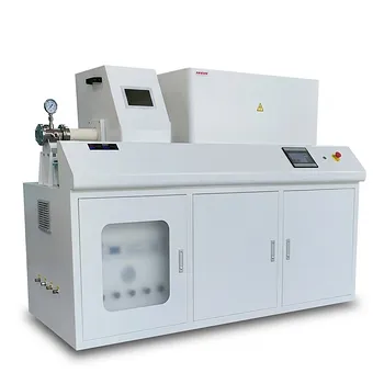
- RF PECVD System Radio Frequency Plasma-Enhanced Chemical Vapor Deposition RF PECVD
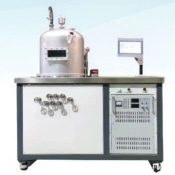
- Chemical Vapor Deposition CVD Equipment System Chamber Slide PECVD Tube Furnace with Liquid Gasifier PECVD Machine
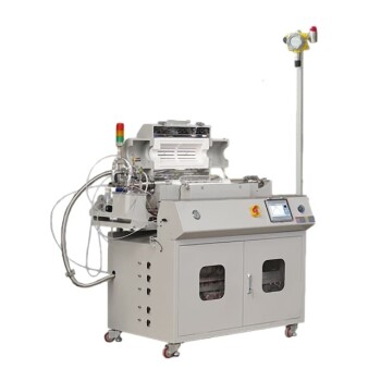
- HFCVD Machine System Equipment for Drawing Die Nano-Diamond Coating
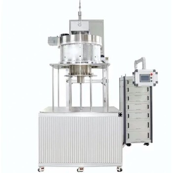
- Customer Made Versatile CVD Tube Furnace Chemical Vapor Deposition Chamber System Equipment
- 915MHz MPCVD Diamond Machine Microwave Plasma Chemical Vapor Deposition System Reactor
People Also Ask
- What is plasma enhanced chemical Vapour deposition process used for fabrication of? A Guide to Low-Temperature Thin Films
- How does plasma enhance CVD? Unlock Low-Temperature, High-Quality Film Deposition
- What is plasma enhanced chemical vapour deposition process? Unlock Low-Temperature, High-Quality Thin Films
- What is the role of RF-PECVD in VFG preparation? Mastering Vertical Growth and Surface Functionality
- What is plasma enhanced chemical vapour deposition PECVD used for? Enable Low-Temp Thin Films for Electronics & Solar

