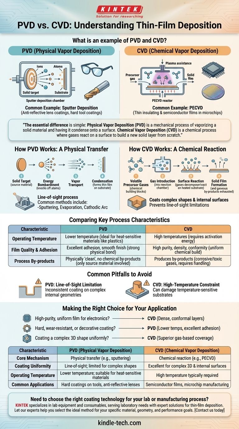
A common example of PVD is sputter deposition, used to apply anti-reflective coatings on eyeglass lenses and protective hard coatings on cutting tools. A common example of CVD is Plasma-Enhanced Chemical Vapor Deposition (PECVD), a critical process used to create the thin insulating and semiconductor films required in microchip manufacturing.
The essential difference is simple: Physical Vapor Deposition (PVD) is a mechanical process of vaporizing a solid material and having it condense onto a surface, like steam fogging a mirror. Chemical Vapor Deposition (CVD) is a chemical process where gases react on a surface to build a new solid layer from scratch.
The Fundamental Difference: Physical vs. Chemical
Understanding the core mechanism of each technique is the key to knowing when and why to use them. They are not interchangeable; they are fundamentally different ways of building a thin film.
How PVD Works: A Physical Transfer
In PVD, a solid source material, known as the target, is bombarded with energy inside a vacuum chamber. This energy physically knocks atoms or molecules off the target, turning them into a vapor.
This vapor then travels in a straight line through the vacuum and condenses on the cooler substrate, forming a thin, solid film. It is a line-of-sight process, meaning the material can only coat surfaces it can "see" from the source.
Common PVD methods include sputtering, evaporation (including electron-beam evaporation), and cathodic arc deposition.
How CVD Works: A Chemical Reaction
CVD begins with introducing one or more volatile precursor gases into a reaction chamber containing the substrate. It is not the final coating material that is introduced, but its chemical building blocks.
These gases decompose or react with each other on the heated substrate's surface. This chemical reaction forms the desired solid film, and any gaseous by-products are exhausted from the chamber.
Because the process is driven by gas molecules, CVD can coat complex shapes and internal surfaces much more uniformly, as the gas can reach areas not in the direct line of sight.
Comparing Key Process Characteristics
The difference between a physical transfer and a chemical reaction creates distinct advantages and disadvantages for each method.
Operating Temperature
PVD is generally a lower-temperature process. This makes it ideal for coating materials that cannot withstand high heat, such as plastics or certain metal alloys.
CVD typically requires high temperatures to provide the necessary activation energy for the chemical reactions to occur on the substrate surface.
Film Quality and Adhesion
PVD films are known for having excellent adhesion and a very smooth surface finish. The energy of the depositing atoms can create a very strong bond with the substrate.
CVD films are often characterized by their high purity, density, and excellent conformity. The chemical reaction builds a very uniform, high-quality layer, which is why it is so prevalent in the semiconductor industry.
Process By-products
PVD is a physically "clean" process. The only material involved is the source material being deposited, so there are no chemical by-products to manage.
CVD, by its nature, produces by-products from the chemical reaction. These can be corrosive or toxic gases that require careful handling and disposal.
Common Pitfalls to Avoid
Choosing the wrong method for an application can lead to film failure, damaged substrates, or unnecessary expense. The trade-offs are significant.
The Line-of-Sight Limitation of PVD
A common mistake is specifying PVD for a part with complex internal geometry or deep, narrow features. The line-of-sight nature of PVD means these areas will receive little to no coating, leading to inconsistent performance.
The High-Temperature Constraint of CVD
Attempting to use a traditional high-temperature CVD process on a temperature-sensitive substrate is a frequent error. This can warp, melt, or otherwise destroy the part you are trying to coat.
Making the Right Choice for Your Application
Your final decision must be driven by the specific requirements of the film and the limitations of the material being coated.
- If your primary focus is a high-purity, uniform film for electronics: CVD is almost always the correct choice for its ability to create dense, conformal layers critical for semiconductor performance.
- If your primary focus is a hard, wear-resistant, or decorative coating on a finished part: PVD is typically preferred for its lower temperatures, excellent adhesion, and wide range of available coating materials.
- If your primary focus is coating a complex 3D shape uniformly: CVD's gas-based process provides superior coverage over the line-of-sight limitations inherent in most PVD techniques.
Ultimately, selecting the right deposition technology begins with a clear understanding of your material, your geometry, and your desired outcome.
Summary Table:
| Characteristic | PVD (Physical Vapor Deposition) | CVD (Chemical Vapor Deposition) |
|---|---|---|
| Core Mechanism | Physical transfer of material (e.g., sputtering) | Chemical reaction on the surface (e.g., PECVD) |
| Coating Uniformity | Line-of-sight; limited for complex shapes | Excellent for complex 3D shapes and internal surfaces |
| Operating Temperature | Lower temperature; suitable for heat-sensitive materials | High temperature typically required |
| Common Applications | Hard coatings on tools, anti-reflective lenses | Semiconductor films, microchip manufacturing |
Need to choose the right coating technology for your lab or manufacturing process? The choice between PVD and CVD is critical for achieving the desired film properties, from wear resistance to high-purity semiconductor layers. KINTEK specializes in lab equipment and consumables, serving laboratory needs with expert solutions for thin-film deposition. Let our experts help you select the ideal method for your specific material, geometry, and performance goals. Contact us today to discuss your application!
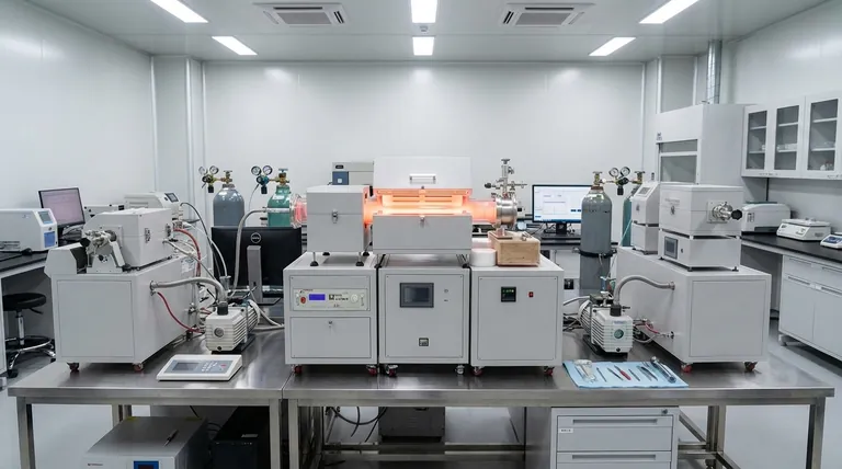
Visual Guide
Related Products
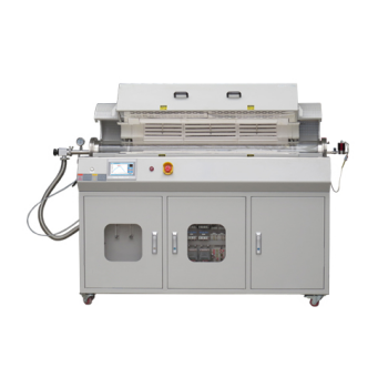
- Chemical Vapor Deposition CVD Equipment System Chamber Slide PECVD Tube Furnace with Liquid Gasifier PECVD Machine
- Inclined Rotary Plasma Enhanced Chemical Vapor Deposition PECVD Equipment Tube Furnace Machine
- RF PECVD System Radio Frequency Plasma-Enhanced Chemical Vapor Deposition RF PECVD
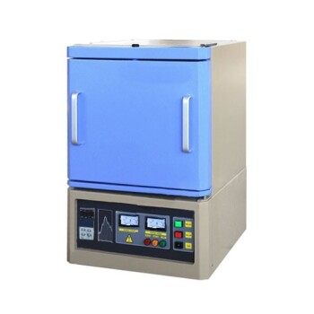
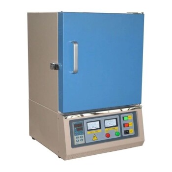
- Customer Made Versatile CVD Tube Furnace Chemical Vapor Deposition Chamber System Equipment
- Vacuum Hot Press Furnace Machine for Lamination and Heating
People Also Ask
- What is the precursor gas in PECVD? The Key to Low-Temperature Thin Film Deposition
- How is PECVD different from CVD? Unlock Low-Temperature Thin Film Deposition
- What is the difference between CVD and PVD process? A Guide to Choosing the Right Coating Method
- How are PECVD and CVD different? A Guide to Choosing the Right Thin-Film Deposition Process
- Why is PECVD better than CVD? Achieve Superior Low-Temperature Thin Film Deposition