A classic example is the ultra-thin, invisible metallic coating on modern energy-efficient windows. That coating, which reflects heat to keep buildings cooler in the summer and warmer in the winter, is applied using a process called sputtering. It is a precise method of depositing a thin film of material onto a surface, atom by atom.
Sputtering is not a material, but a physical process used to create high-performance coatings. Think of it as a microscopic form of sandblasting where ejected atoms from a source material are deposited to form an exceptionally thin and uniform layer on a target object.
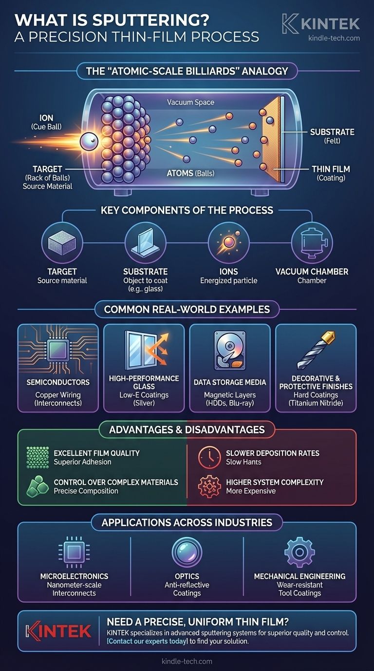
What is Sputtering? A Foundational Analogy
At its core, sputtering is a type of Physical Vapor Deposition (PVD). It takes place inside a vacuum chamber to ensure purity and control. The simplest way to visualize it is with a game of atomic-scale billiards.
The Billiards Analogy
Imagine a rack of billiard balls as your source material, called the target (e.g., a solid block of silver). The felt of the table is the object you want to coat, called the substrate (e.g., a pane of glass).
Now, you shoot a high-energy cue ball—an energized particle called an ion—into the rack. The impact is so forceful that it doesn't just break the rack; it knocks individual billiard balls (atoms) completely off the table.
These ejected atoms fly across the vacuum and stick to the felt, the substrate. If you do this millions of times from every angle, you will eventually build up a perfectly uniform, one-atom-thick layer of "billiard balls" across the entire table. This is the thin film.
Key Components of the Process
- Target: The source material you wish to deposit (e.g., titanium, gold, silver, aluminum).
- Substrate: The object you are coating (e.g., a silicon wafer, a piece of glass, a plastic part).
- Ions: Typically, atoms of an inert gas like Argon are energized to become the "sandblasting" particles that bombard the target.
- Vacuum Chamber: The entire process occurs in a near-vacuum to prevent contamination from air particles and allow the sputtered atoms to travel freely.
Common Real-World Examples of Sputtering
This precise control over thin film deposition makes sputtering a cornerstone of modern technology.
Semiconductor Manufacturing
The microscopic copper wiring that connects billions of transistors inside a computer chip is created using sputtering. This process ensures the conductive layers are pure, uniform, and adhere perfectly to the silicon wafer.
High-Performance Glass Coatings
Low-emissivity (Low-E) windows use sputtered layers of silver to reflect infrared light (heat). Anti-reflective coatings on eyeglasses and camera lenses also use sputtering to deposit multiple layers of materials like silicon dioxide and titanium dioxide.
Data Storage Media
The magnetic layers on a computer's hard disk platter, which store your data, are deposited through sputtering. Similarly, the reflective layer on a Blu-ray disc or DVD is often a sputtered aluminum alloy.
Decorative & Protective Finishes
The durable, gold-colored coating on high-end drill bits is often Titanium Nitride (TiN), applied via sputtering. This hard ceramic layer reduces friction and wear. Many "chrome-look" plastics on cars and electronics also get their metallic finish from this process.
Understanding the Trade-offs
Sputtering is an invaluable technique, but it is chosen for specific reasons and has clear trade-offs compared to other deposition methods like thermal evaporation.
Advantage: Excellent Film Quality
Sputtered atoms have higher kinetic energy than evaporated ones. This energy helps them form a denser, more uniform, and more strongly bonded film on the substrate, resulting in superior adhesion and durability.
Advantage: Control Over Complex Materials
Sputtering is excellent for depositing alloys and compounds. The "sandblasting" nature of the process ejects atoms from the target in the same ratio they exist, allowing you to create a thin film with the same chemical composition as the source.
Disadvantage: Slower Deposition Rates
Generally, sputtering is a slower process than thermal evaporation. For applications where thick films are needed quickly and ultimate density isn't critical, other methods might be more economical.
Disadvantage: Higher System Complexity
Sputtering systems, with their need for high-voltage power supplies and gas management, are typically more complex and expensive than simple evaporation systems. The process also generates more heat, which can be a concern for delicate substrates.
How Sputtering Applies Across Industries
Understanding the purpose of sputtering helps you recognize its role in the products you use every day. Your decision to use it depends entirely on the goal.
- If your primary focus is microelectronics: Sputtering is the industry standard for creating the reliable, nanometer-scale metallic interconnects and barrier layers inside integrated circuits.
- If your primary focus is optics: Sputtering provides the precise, multi-layer control needed to create advanced anti-reflective, reflective, or filtering coatings on lenses and glass.
- If your primary focus is mechanical engineering: Sputtering is used to apply hard, wear-resistant coatings (like TiN) that dramatically extend the life and performance of tools and components.
By understanding this foundational manufacturing process, you gain insight into how countless high-performance products are made possible.
Summary Table:
| Application | Sputtered Material | Purpose |
|---|---|---|
| Energy-Efficient Windows | Silver | Reflects infrared heat (Low-E coating) |
| Semiconductor Chips | Copper | Creates microscopic conductive wiring |
| Hard Coatings (e.g., Drill Bits) | Titanium Nitride (TiN) | Provides extreme wear resistance |
| Anti-Reflective Lenses | Silicon Dioxide, Titanium Dioxide | Reduces glare on eyeglasses and camera lenses |
Need a precise, uniform thin film for your application? The sputtering process is ideal for creating high-performance coatings on semiconductors, optical components, and industrial tools. At KINTEK, we specialize in advanced lab equipment, including sputtering systems, to help you achieve superior film quality, excellent adhesion, and precise control over complex materials. Let's discuss your project requirements – contact our experts today to find the perfect solution for your laboratory needs.
Visual Guide
Related Products
- Lab Sterile Slapping Type Homogenizer for Tissue Mashing and Dispersing
- Spark Plasma Sintering Furnace SPS Furnace
- Single Punch Manual Tablet Press Machine TDP Tablet Punching Machine
People Also Ask
- What role does an ultrasonic cleaner play in the pre-treatment of 4140 steel? Ensure Uniform Nitriding Activation
- How do ultrasonic cell disruptors or dispersion equipment function during ZIF-8 synthesis? Master Acoustic Cavitation
- What role does a laboratory homogenizer play in radioactive cesium detection? Ensure Accuracy in Wildlife Sampling
- Why is it necessary to use an ultrasonic cell disruptor before yeast flow cytometry? Ensure Data Accuracy
- How do lab stirrers & homogenizers ensure uniform distribution? Optimize Your Complex Multiphase Chemical Mixing


