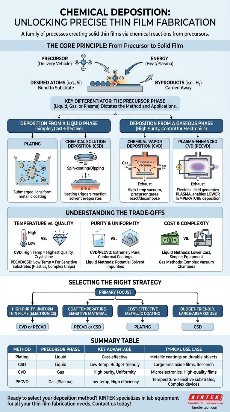
In short, chemical deposition is a family of processes used to create a solid, thin film on a surface (known as a substrate) by initiating a chemical reaction. Instead of simply spraying or melting a material on, these methods use chemical "precursors" that react at the substrate to build the desired material, often one layer of atoms at a time. This allows for precise control over the film's thickness, purity, and properties.
The most important concept to grasp is that the primary difference between various chemical deposition techniques lies in the physical state—or phase—of the chemical precursor used. Whether you start with a liquid, a gas, or an energized gas (plasma) dictates the entire method and its applications.
The Core Principle: From Precursor to Solid Film
To understand chemical deposition, you must first understand the role of the precursor. It's the foundational concept that ties all these methods together.
What is a Precursor?
A precursor is a chemical compound that contains the atoms you want to deposit, but in a volatile or soluble form. Think of it as the delivery vehicle for your desired atoms.
For example, to deposit a film of pure silicon (Si), you wouldn't use a block of solid silicon. Instead, you might use a precursor gas like silane (SiH₄), which carries the silicon atom in a form that can be easily transported and reacted.
The Role of Chemical Reactions
The deposition process is not physical; it is inherently chemical. Energy—typically in the form of heat or plasma—is applied to the precursor at the substrate's surface.
This energy breaks the chemical bonds in the precursor molecules. The desired atoms (like silicon) bond to the substrate, while the unwanted byproduct molecules (like hydrogen gas) are carried away.
Deposition from a Liquid Phase
These methods begin with a precursor dissolved in a liquid solution. They are often simpler and less expensive than gas-phase techniques.
Plating
Plating involves submerging the substrate in a liquid chemical bath. A chemical reaction in the solution causes ions of the desired material (e.g., nickel, copper, gold) to form a solid metallic coating on the object's surface. This is the oldest form of chemical deposition.
Chemical Solution Deposition (CSD)
In CSD, a liquid solution containing the precursor is coated onto a substrate, often by spinning it at high speed (spin-coating) or dipping it. The substrate is then heated. This heating process evaporates the solvent and triggers a chemical reaction that transforms the precursor into the final solid film.
Deposition from a Gaseous Phase
Gas-phase methods are the workhorse of the modern electronics industry. They offer exceptionally high purity and control, which is essential for manufacturing microchips.
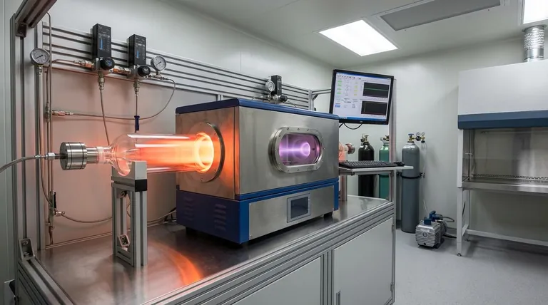
Chemical Vapor Deposition (CVD)
In a CVD process, precursor gases are introduced into a high-temperature vacuum chamber. When these hot gases come into contact with the substrate, they react and decompose, leaving behind a highly pure and uniform thin film.
Plasma-Enhanced CVD (PECVD)
PECVD is a crucial evolution of CVD. Instead of relying solely on high heat, this method uses an electrical field to generate a plasma—an energized, reactive gas.
The plasma helps break down the precursor gas molecules much more efficiently. This allows the deposition to occur at significantly lower temperatures, which is critical for building complex devices with layers that cannot withstand the intense heat of traditional CVD.
Understanding the Trade-offs
No single method is universally superior. The choice depends entirely on the material being deposited, the substrate it's being deposited on, and the desired quality of the final film.
Temperature vs. Quality
High-temperature processes like conventional CVD often produce the highest-quality, most crystalline films. However, this intense heat can damage or warp many substrates. Low-temperature PECVD and CSD provide a way to coat sensitive materials like plastics or complex electronic chips.
Purity and Uniformity
Gas-phase methods (CVD and PECVD) excel at creating films that are extremely pure and can conformally coat even the most complex 3D structures. Liquid-phase methods can sometimes struggle with impurities left over from the solvent.
Cost and Complexity
Generally, liquid-phase processes like plating and CSD are less expensive and use simpler equipment than the complex vacuum chambers required for CVD and PECVD. This makes them ideal for large-area coatings where ultimate purity isn't the primary concern.
Selecting the Right Deposition Strategy
Choosing a method requires balancing your technical needs with practical constraints.
- If your primary focus is high-purity, uniform thin films for electronics: Your default choice will be Chemical Vapor Deposition (CVD) or its plasma-enhanced variant (PECVD).
- If you need to coat a temperature-sensitive material: Plasma-Enhanced CVD (PECVD) or a liquid-phase method like Chemical Solution Deposition (CSD) offers a crucial low-temperature advantage.
- If your goal is a cost-effective metallic coating on a durable object: Traditional plating methods offer a robust and scalable solution.
- If you are developing new oxide films for research or large-area applications on a budget: Chemical Solution Deposition (CSD) provides an accessible and versatile starting point.
By understanding the state of the precursor, you can effectively navigate these powerful techniques and select the right tool for your material science challenge.
Summary Table:
| Method | Precursor Phase | Key Advantage | Typical Use Case |
|---|---|---|---|
| Plating | Liquid | Cost-effective | Metallic coatings on durable objects |
| Chemical Solution Deposition (CSD) | Liquid | Low-temperature, budget-friendly | Large-area oxide films, research |
| Chemical Vapor Deposition (CVD) | Gas | High purity, uniformity | Microelectronics, high-quality films |
| Plasma-Enhanced CVD (PECVD) | Gas (Plasma) | Low-temperature, high efficiency | Temperature-sensitive substrates, complex devices |
Ready to select the perfect deposition method for your project? KINTEK specializes in lab equipment and consumables for all your thin-film fabrication needs. Whether you're working with CVD, PECVD, or solution-based methods, our expertise ensures you get the right tools for precise, high-quality results. Contact us today to discuss your specific application and discover how we can enhance your laboratory's capabilities!
Visual Guide
Related Products
- Chemical Vapor Deposition CVD Equipment System Chamber Slide PECVD Tube Furnace with Liquid Gasifier PECVD Machine
- Microwave Plasma Chemical Vapor Deposition MPCVD Machine System Reactor for Lab and Diamond Growth
- 915MHz MPCVD Diamond Machine Microwave Plasma Chemical Vapor Deposition System Reactor
- Customer Made Versatile CVD Tube Furnace Chemical Vapor Deposition Chamber System Equipment
- Split Chamber CVD Tube Furnace with Vacuum Station Chemical Vapor Deposition System Equipment Machine
People Also Ask
- How expensive is chemical vapor deposition? Understanding the True Cost of High-Performance Coating
- What is the chemical vapor deposition growth process? Build Superior Thin Films from the Atom Up
- What happens during deposition chemistry? Building Thin Films from Gaseous Precursors
- What are the processes of vapor phase deposition? Understand CVD vs. PVD for Superior Thin Films
- What types of substrates are used in CVD to facilitate graphene films? Optimize Graphene Growth with the Right Catalyst


