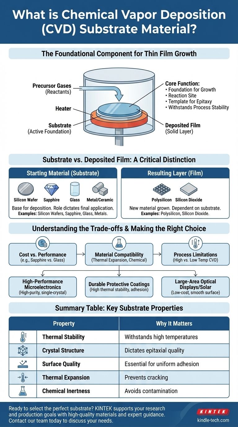
In chemical vapor deposition (CVD), the substrate is the foundational material or surface upon which a thin film is grown. It acts as the physical base where gaseous chemical precursors react to form a solid layer. While materials like polysilicon and silicon dioxide are produced using CVD, they are typically the film being deposited, not the substrate itself.
The substrate is not merely a passive holder; it is an active component in the CVD process. Its physical and chemical properties—such as crystal structure, thermal stability, and surface quality—are critical because they directly dictate the quality, structure, and performance of the final deposited film.
The Core Function of the Substrate
A substrate serves as the template and reaction site for the entire deposition process. Understanding its role is fundamental to understanding CVD.
A Foundation for Growth
The substrate provides the necessary surface area for the chemical reactions to occur. The precursor gases are introduced into a chamber containing the heated substrate, and the film begins to form molecule by molecule directly on its surface.
Controlling Film Properties
For many advanced applications, the atomic arrangement of the substrate is paramount. The substrate's crystal lattice can act as a template, guiding the deposited film to grow with a similar, highly ordered structure in a process called epitaxy.
Ensuring Process Stability
The CVD process often involves very high temperatures and reactive chemicals. The substrate must be able to withstand these harsh conditions without melting, warping, or reacting undesirably with the precursor gases.
Substrate vs. Deposited Film: A Critical Distinction
A common point of confusion is the difference between the material you start with (the substrate) and the material you create (the film).
The Starting Material (The Substrate)
This is the base component placed into the CVD reactor. The choice of substrate depends entirely on the final application. Common examples include:
- Silicon Wafers: The bedrock of the semiconductor industry.
- Sapphire: Used for high-performance LEDs and specialized electronics.
- Glass or Quartz: Common for displays and optical components.
- Metals and Ceramics: Used for creating hard, protective coatings on tools.
The Resulting Layer (The Film)
This is the new material grown on top of the substrate. The materials mentioned in the references are excellent examples of films.
- Polysilicon: A film often deposited onto a substrate for solar panel manufacturing.
- Silicon Dioxide: A film grown on a silicon wafer to act as an electrical insulator in microchips.
Understanding the Trade-offs
Selecting a substrate is an exercise in balancing performance requirements with practical limitations. Making the wrong choice can compromise the entire process.
Cost vs. Performance
The highest-quality substrates, like single-crystal sapphire or silicon carbide, are extremely expensive. For less demanding applications, a more cost-effective substrate like glass or a lower-grade silicon wafer may be sufficient, even if it results in a less-perfect film.
Material Compatibility
The substrate and the film must be chemically and physically compatible. A primary concern is the thermal expansion coefficient. If the substrate and film expand and contract at different rates during heating and cooling, the immense stress can cause the film to crack or peel off.
Process Limitations
The properties of the substrate can restrict which CVD techniques you can use. For instance, a substrate with a low melting point cannot be used in a high-temperature thermal CVD process, forcing the use of a lower-temperature method like plasma-enhanced CVD (PECVD).
Making the Right Choice for Your Goal
The ideal substrate is always defined by the intended use of the final product.
- If your primary focus is high-performance microelectronics: Your choice must be a high-purity, single-crystal substrate like a silicon wafer to ensure the flawless epitaxial growth of semiconductor films.
- If your primary focus is a durable, protective coating: The key is a substrate with excellent thermal stability and surface adhesion properties, such as a steel or ceramic tool bit.
- If your primary focus is large-area optical displays or solar cells: Your decision will be driven by finding a low-cost substrate, like glass or specialized polymers, that provides a smooth, stable surface.
Ultimately, choosing the right substrate is as critical as the deposition chemistry itself, as it defines the foundation upon which your final product is built.
Summary Table:
| Property | Why It Matters for CVD Substrates |
|---|---|
| Thermal Stability | Must withstand high process temperatures without degrading. |
| Crystal Structure | Dictates the quality of epitaxial film growth (e.g., for semiconductors). |
| Surface Quality | A smooth, clean surface is essential for uniform film adhesion. |
| Thermal Expansion | Must be compatible with the film to prevent cracking or delamination. |
| Chemical Inertness | Should not react with precursor gases, which would contaminate the film. |
Ready to select the perfect substrate for your CVD application? The right foundation is critical to your project's success. KINTEK specializes in providing high-quality lab equipment and consumables, including substrates and CVD systems, to meet the precise needs of your laboratory. Our experts can help you navigate material compatibility and process requirements to ensure optimal results. Contact our team today to discuss your specific needs and discover how we can support your research and production goals.
Visual Guide
Related Products
- Custom CVD Diamond Coating for Lab Applications
- CVD Diamond for Thermal Management Applications
- Chemical Vapor Deposition CVD Equipment System Chamber Slide PECVD Tube Furnace with Liquid Gasifier PECVD Machine
- 915MHz MPCVD Diamond Machine Microwave Plasma Chemical Vapor Deposition System Reactor
- HFCVD Machine System Equipment for Drawing Die Nano-Diamond Coating
People Also Ask
- What are the different CVD coating? A Guide to Thermal CVD, PECVD, and Specialized Methods
- What is CVD diamond coating? Grow a Super-Hard, High-Performance Diamond Layer
- What are the advantages of CVD coating? Superior Hardness and Uniformity for Demanding Applications
- What is the use of CVD coating? Enhance Durability and Functionality for Your Components
- What is CVD coated? A Guide to Superior Wear Resistance for Complex Parts