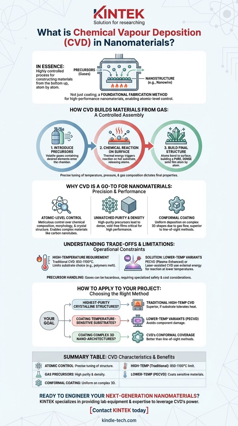
In essence, Chemical Vapor Deposition (CVD) is a highly controlled process for constructing materials, including nanomaterials, from the bottom up. It involves introducing reactive gases (precursors) into a chamber where they decompose and deposit onto a heated surface (substrate), forming a high-purity solid film or structure like a nanowire.
CVD is not just a coating technique; it is a foundational fabrication method for high-performance nanomaterials. Its primary strength lies in its exceptional ability to control the structure, purity, and properties of materials at the atomic level, making it indispensable for advanced electronics and materials science.
How CVD Builds Materials from Gas
To understand why CVD is so crucial for nanomaterials, we must first look at its fundamental mechanism. It's a process of controlled assembly, not just application.
The Core Principle: A Chemical Reaction on a Surface
The process begins by introducing one or more volatile precursor gases into a reaction chamber. These gases contain the elements you want to deposit.
When these gases come into contact with a heated substrate, the thermal energy triggers a chemical reaction. This reaction breaks down the precursor molecules, releasing the desired atoms.
The Role of the Substrate
The substrate serves as the foundation upon which the new material grows. Its temperature is a critical parameter that dictates the rate and nature of the chemical reaction.
The atoms freed from the gas precursors then bond to this heated surface, creating a stable, solid layer.
Building the Final Structure
Over time, this process builds up a solid film atom by atom. Because it's built from the gas phase, the material can be exceptionally pure and dense.
By precisely tuning the process parameters—like temperature, pressure, and gas composition—engineers can dictate the final material's properties, from its crystal structure to its thickness.
Why CVD is a Go-To for Nanomaterials
The unique characteristics of the CVD process make it exceptionally well-suited for the demanding world of nanotechnology, where precision is paramount.
Atomic-Level Control
CVD allows for meticulous control over the final product. Adjusting deposition parameters enables the fabrication of materials with a specific chemical composition, morphology, and crystal structure. This is how materials like single-walled carbon nanotubes or precisely structured GaN nanowires are grown.
Unmatched Purity and Density
Because the precursors are in a gaseous state, it's possible to use highly refined sources, leading to final materials of very high purity. The atom-by-atom deposition also results in films that are incredibly dense and free from voids, which is critical for high-performance applications.
Conformal Coating on Complex Shapes
One of CVD's most significant advantages is its ability to create conformal coatings. Since the gas precursors flow around an object, the deposition occurs evenly on all surfaces. This "wrap-around" effect is essential for coating complex, three-dimensional nanostructures where line-of-sight methods would fail.
Understanding the Trade-offs and Limitations
No process is perfect. To use CVD effectively, you must understand its operational constraints and when a different approach might be necessary.
The High-Temperature Requirement
The most significant limitation of traditional CVD is the high reaction temperature, often between 850-1100°C. Many substrate materials, particularly polymers or certain pre-processed electronic components, cannot withstand this heat without melting or being damaged.
The Solution: Lower-Temperature Variants
To overcome the heat limitation, variants have been developed. Techniques like Plasma-Enhanced CVD (PECVD) or laser-assisted CVD use an external energy source (plasma or a laser) to initiate the chemical reaction, allowing deposition to occur at much lower temperatures.
Precursor Handling and Cost
The precursor gases used in CVD can be expensive, toxic, corrosive, or flammable. This necessitates specialized handling procedures and safety equipment, which can add to the overall cost and complexity of the operation.
How to Apply This to Your Project
Your choice of fabrication method depends entirely on the material requirements and substrate limitations of your specific goal.
- If your primary focus is producing the highest-purity crystalline structures (like single-walled carbon nanotubes): Traditional, high-temperature CVD is often the superior method, provided your substrate can tolerate the heat.
- If your primary focus is coating temperature-sensitive substrates (like polymers or certain electronics): You must explore lower-temperature variants like Plasma-Enhanced CVD (PECVD) to avoid damaging your component.
- If your primary focus is coating complex, three-dimensional nano-architectures: CVD's excellent conformal coverage makes it a far better choice than line-of-sight methods like sputtering or evaporation.
Ultimately, mastering CVD is about leveraging its precise control to engineer the materials of the future, one layer at a time.
Summary Table:
| CVD Characteristic | Benefit for Nanomaterials |
|---|---|
| Atomic-Level Control | Precise tuning of composition, morphology, and crystal structure (e.g., carbon nanotubes). |
| Gas-Phase Precursors | Enables exceptionally high-purity and dense final materials. |
| Conformal Coating | Uniform deposition on complex 3D nanostructures, unlike line-of-sight methods. |
| High-Temperature Requirement | Traditional CVD requires 850-1100°C, limiting substrate choice. |
| Lower-Temperature Variants (e.g., PECVD) | Enables coating of temperature-sensitive materials like polymers. |
Ready to Engineer Your Next-Generation Nanomaterials with Precision?
Chemical Vapor Deposition is the key to unlocking the high-purity, high-performance materials required for cutting-edge applications in electronics, photonics, and advanced materials science. KINTEK specializes in providing the lab equipment and expertise necessary to leverage CVD's power for your specific project.
Whether you are growing carbon nanotubes, depositing thin films on complex 3D structures, or need a solution for temperature-sensitive substrates, our team can help you select the right system and optimize your process.
Contact KINTEK today to discuss how our specialized lab equipment and consumables can help you achieve unparalleled control and quality in your nanomaterial fabrication.
Visual Guide
Related Products
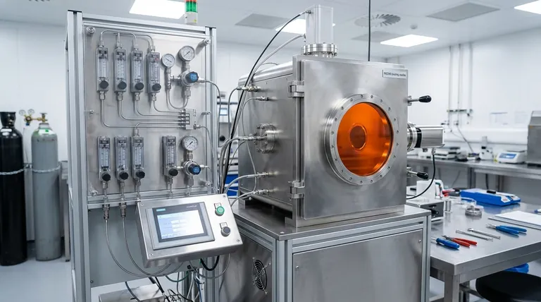
- Chemical Vapor Deposition CVD Equipment System Chamber Slide PECVD Tube Furnace with Liquid Gasifier PECVD Machine
- Microwave Plasma Chemical Vapor Deposition MPCVD Machine System Reactor for Lab and Diamond Growth
- 915MHz MPCVD Diamond Machine Microwave Plasma Chemical Vapor Deposition System Reactor
- Customer Made Versatile CVD Tube Furnace Chemical Vapor Deposition Chamber System Equipment
- HFCVD Machine System Equipment for Drawing Die Nano-Diamond Coating
People Also Ask
- How expensive is chemical vapor deposition? Understanding the True Cost of High-Performance Coating
- What happens during deposition chemistry? Building Thin Films from Gaseous Precursors
- Why is Chemical Vapor Deposition (CVD) equipment uniquely suited for constructing hierarchical superhydrophobic structures?
- What are the core advantages of PE-CVD in OLED encapsulation? Protect Sensitive Layers with Low-Temp Film Deposition
- What are the advantages of chemical vapor deposition? Achieve Superior Thin Films for Your Lab


