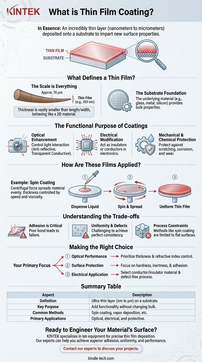
In essence, a thin film coating is an incredibly thin layer of material, ranging from fractions of a nanometer to several micrometers thick, that is intentionally deposited onto the surface of another material (known as a substrate). This process is not merely for coverage; its purpose is to grant the substrate's surface entirely new properties, such as enhanced durability, altered electrical conductivity, or specialized optical performance.
The fundamental purpose of a thin film coating is to fundamentally alter a material's surface properties without changing its bulk structure. By applying this microscopically thin layer, you can give an ordinary object extraordinary capabilities—making glass anti-reflective, a metal tool corrosion-resistant, or a semiconductor functional.
What Defines a Thin Film?
A thin film is distinct from a simple layer of paint or plating due to its extreme thinness. This dimensional characteristic is the source of its unique properties.
The Scale is Everything
A thin film is a layer of material where its thickness is vastly smaller than its length and width. We are often talking about layers measured in nanometers (billionths of a meter) or micrometers (millionths of a meter).
Because this third dimension (thickness) is so suppressed, the film behaves almost like a two-dimensional material, where surface effects and quantum phenomena can become dominant.
The Substrate Foundation
The thin film is always applied to a substrate, which is the underlying material or object being coated. This could be anything from a silicon wafer for electronics, a piece of glass for an optical lens, or a metal component for an engine.
The final product combines the bulk properties of the substrate (like strength or shape) with the specialized surface properties of the film.
The Functional Purpose of Coatings
Thin film coatings are applied to achieve a specific functional outcome. The material and deposition method are chosen to impart a desired characteristic onto the substrate's surface.
Optical Enhancement
Coatings can be engineered to control the way light interacts with a surface. This includes creating transparent conductive layers for touch screens or making camera lenses anti-reflective to maximize light transmission.
Electrical Modification
Thin films are critical in electronics. They can act as electrical insulators to separate conductive paths in an integrated circuit or serve as the conductive pathways themselves.
Mechanical and Chemical Protection
A primary use for thin films is to protect the underlying substrate. Coatings can provide exceptional scratch resistance, increase surface durability, or create a barrier that offers powerful corrosion resistance.
How Are These Films Applied?
There are numerous methods for depositing a thin film, but they all involve carefully controlled processes to achieve a uniform layer with a precise thickness.
The Principle of Deposition
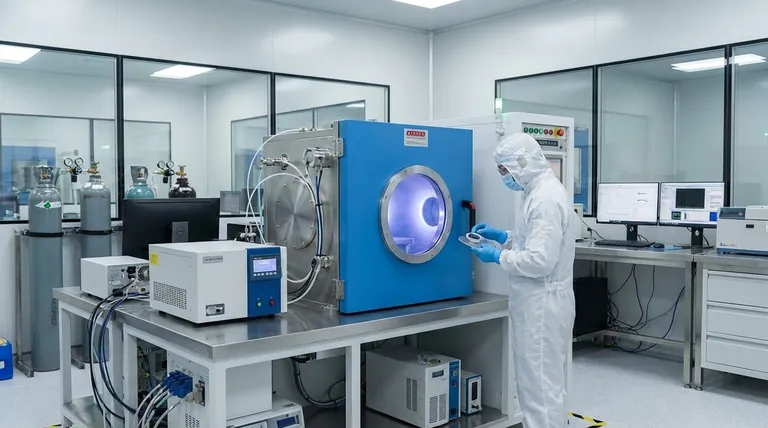
Deposition is the process of applying the coating material atom by atom or molecule by molecule onto the substrate. This can be done from a vapor, a liquid, or a plasma.
Example: Spin Coating
A common method for flat substrates is spin coating. A small amount of the coating material in liquid form is placed in the center of the substrate.
The substrate is then spun at a very high speed. Centrifugal force spreads the liquid evenly across the surface, and the excess material flies off. The final thickness is precisely controlled by the spinning speed and the viscosity of the liquid.
Understanding the Trade-offs
While powerful, thin film coating technology involves critical challenges and limitations that must be managed.
Adhesion is Critical
A thin film is only as effective as its bond to the substrate. Poor adhesion can lead to the coating peeling, flaking, or blistering, completely negating its benefits.
Uniformity and Defects
Achieving a perfectly uniform thickness across the entire surface is a significant engineering challenge. Pinholes, cracks, or contaminants in the film can create points of failure, especially in electronic or protective applications.
Process Constraints
The method of deposition places limits on the application. For example, spin coating works exceptionally well for flat, round substrates like wafers but is unsuitable for coating complex, three-dimensional objects.
Making the Right Choice for Your Goal
The ideal thin film strategy depends entirely on the problem you are trying to solve.
- If your primary focus is optical performance: You must prioritize materials and deposition methods that give you precise control over thickness and the material's refractive index.
- If your primary focus is surface protection: Your main concerns will be the coating's intrinsic hardness, its chemical inertness, and ensuring excellent adhesion to the substrate.
- If your primary focus is an electrical application: The choice of material (conductor or insulator) is paramount, and the process must guarantee a continuous, defect-free layer.
Ultimately, thin film technology allows you to engineer the surface of a material with the same precision you use to engineer its core.
Summary Table:
| Aspect | Description |
|---|---|
| Definition | An ultra-thin layer (nanometers to micrometers) deposited on a substrate to alter its surface properties. |
| Key Purpose | To add new functionality (e.g., optical, electrical, protective) without changing the substrate's bulk material. |
| Common Methods | Includes spin coating, vapor deposition, and other precise, atom-by-atom application processes. |
| Primary Applications | Optical enhancement (anti-reflective coatings), electronics (conductive layers), and protection (scratch/corrosion resistance). |
Ready to Engineer Your Material's Surface with Precision?
Thin film coatings are the key to unlocking advanced functionality in your products, from enhancing optical clarity to providing robust protection. KINTEK specializes in lab equipment and consumables for thin film deposition, serving the precise needs of research and development laboratories.
Our expertise can help you select the right coating materials and methods to achieve superior adhesion, uniformity, and performance for your specific application.
Contact our experts today to discuss how we can support your thin film projects and bring your material innovations to life.
Visual Guide
Related Products
- Aluminized Ceramic Evaporation Boat for Thin Film Deposition
- Electron Beam Evaporation Coating Oxygen-Free Copper Crucible and Evaporation Boat
- Tungsten Evaporation Boat for Thin Film Deposition
- Molybdenum Tungsten Tantalum Evaporation Boat for High Temperature Applications
- Aluminum-Plastic Flexible Packaging Film for Lithium Battery Packaging
People Also Ask
- Why is an alumina boat and Ti3AlC2 powder bed necessary for Ti2AlC sintering? Protect MAX Phase Purity
- What are the applications of thin films deposition? Unlock New Possibilities for Your Materials
- Why is an alumina boat selected for catalyst precursors? Ensure Sample Purity at 1000 °C
- What is the chemical method for thin film deposition? Build Films from the Molecular Level Up
- Why are high-purity ceramic boats used for lignin activation? Ensure Purity & Thermal Stability


