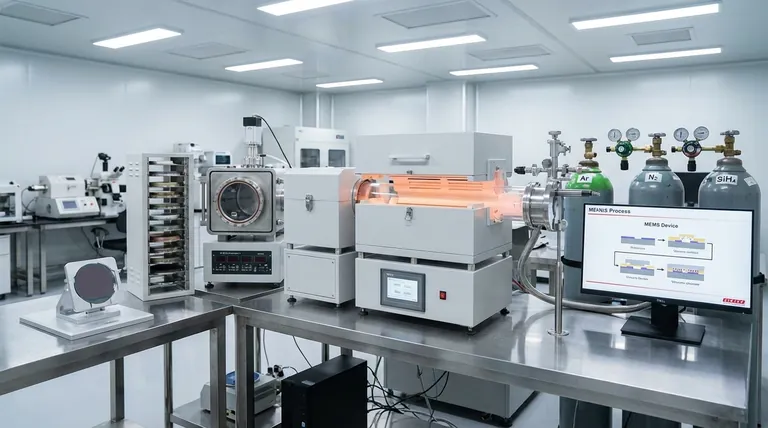
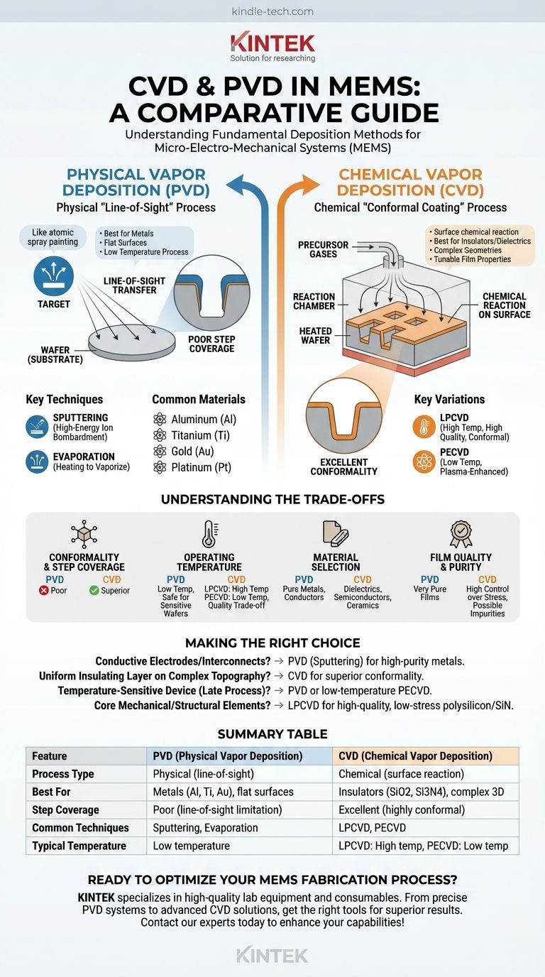
At their core, PVD and CVD are the two fundamental methods used in Micro-Electro-Mechanical Systems (MEMS) manufacturing to deposit thin layers of material onto a substrate. Physical Vapor Deposition (PVD) is a "line-of-sight" physical process, akin to spray painting, where a material is physically transferred onto a wafer. Chemical Vapor Deposition (CVD), by contrast, is a chemical process where gases react on the wafer's surface to grow a new material layer, allowing it to conform to complex shapes.
The critical distinction is this: PVD is a physical, line-of-sight process best for depositing metals on flat surfaces. CVD is a chemical process that creates highly uniform, "conformal" coatings ideal for depositing insulating or structural layers over complex, three-dimensional topographies.
Understanding the Role of Thin Films in MEMS
Every MEMS device, from an accelerometer to a micromirror, is built from a stack of precisely patterned thin films. These films serve as the device's functional building blocks.
Deposition processes are how these essential layers are created. The choice between PVD and CVD directly impacts the material properties, device geometry, and ultimately, the performance and reliability of the final MEMS product.
Physical Vapor Deposition (PVD): The "Line-of-Sight" Method
PVD encompasses a set of vacuum deposition techniques that involve physically moving atoms from a source material (a "target") to the wafer (the "substrate").
The Core Principle of PVD
Think of PVD as a highly controlled spray-painting process at the atomic level. In a high-vacuum chamber, atoms are ejected from a solid source and travel in a straight line until they hit the wafer, where they condense and form a film.
Key PVD Techniques in MEMS
The two most common PVD methods are sputtering and evaporation.
Sputtering is the workhorse of PVD. In this process, a plasma of inert gas (like Argon) is created. High-energy ions from this plasma bombard the target, knocking atoms loose. These ejected atoms then coat the wafer.
Evaporation involves heating the source material in a vacuum until it evaporates. The vaporized atoms then travel to the cooler wafer and condense, forming a film. This is simpler than sputtering but offers less control over film properties.
Characteristics of PVD Films
Because it's a line-of-sight process, PVD struggles to coat the sidewalls of deep trenches or complex structures. This is known as poor step coverage. However, it is excellent for depositing very pure films, especially metals.
Common PVD Materials
PVD is the go-to method for depositing metals used for electrodes, reflective mirrors, and electrical interconnects. Common materials include Aluminum (Al), Titanium (Ti), Gold (Au), and Platinum (Pt).
Chemical Vapor Deposition (CVD): The Conformal Coating Method
CVD is fundamentally different from PVD. It doesn't physically transfer material; it creates it on the wafer's surface through a chemical reaction.
The Core Principle of CVD
In a CVD process, precursor gases are introduced into a reaction chamber containing heated wafers. The gases react on the hot surface, depositing a solid film and producing volatile byproducts that are then pumped away. This process is not limited by line-of-sight, allowing it to form perfectly uniform layers over any geometry. This ability is called conformality.
Key CVD Variations
The "best" CVD process depends on the required temperature and film quality.
-
LPCVD (Low-Pressure CVD): This is the gold standard for high-quality, highly conformal films like polysilicon (a key structural material) and silicon nitride (an excellent insulator). It operates at high temperatures (600°C+) and low pressure.
-
PECVD (Plasma-Enhanced CVD): This process uses an energy-rich plasma to allow the chemical reactions to occur at much lower temperatures (typically <400°C). This is critical when depositing films on wafers that already have temperature-sensitive structures or materials (like metals) on them.
Characteristics of CVD Films
The defining characteristic of CVD is its excellent conformality or step coverage. It can create films of uniform thickness on the top, bottom, and sidewalls of the most complex trenches. Film properties like stress and density are highly tunable.
Common CVD Materials
CVD is essential for depositing dielectrics (insulators) and semiconductors. Common materials include Silicon Dioxide (SiO2), Silicon Nitride (Si3N4), and Polysilicon.
Understanding the Trade-offs: PVD vs. CVD
Choosing between PVD and CVD requires weighing their distinct advantages and disadvantages for a specific application.
Conformality and Step Coverage
- CVD is superior. Its chemical nature ensures a uniform coating over any surface topography. This is non-negotiable for insulating layers or structural films in complex MEMS.
- PVD is poor. As a line-of-sight process, it creates thin or non-existent films on sidewalls and in deep trenches.
Operating Temperature
- High-quality LPCVD is a high-temperature process. This can damage or reflow materials like aluminum already present on the wafer.
- PECVD offers a low-temperature CVD option, but often at the cost of lower film quality compared to LPCVD.
- PVD is generally a low-temperature process, making it safe for processing wafers that have already undergone multiple fabrication steps.
Material Selection
- PVD excels at depositing pure metals and some metallic compounds. It is difficult or impossible to use for materials like silicon nitride or polysilicon.
- CVD is the primary method for depositing dielectrics, semiconductors, and ceramics that are formed through chemical reaction.
Film Quality and Purity
- PVD films are typically very pure, as the source material is physically moved to the substrate with minimal contamination.
- CVD films can have impurities, such as hydrogen in PECVD films, which can affect material properties. However, CVD offers exceptional control over film stress, which is critical for MEMS structures.
Making the Right Choice for Your MEMS Device
Your choice is dictated entirely by the function of the layer you are creating and the constraints of your fabrication process.
- If your primary focus is creating conductive electrodes or interconnects: PVD (sputtering) is the standard, most efficient choice for depositing high-purity metals.
- If your primary focus is building a uniform insulating layer over complex topography: CVD is the only viable option due to its superior conformality.
- If your primary focus is depositing a film late in the process on a temperature-sensitive device: Your choice is between PVD or a low-temperature PECVD process.
- If your primary focus is creating the core mechanical or structural elements of the device: LPCVD is often used to deposit high-quality, low-stress polysilicon or silicon nitride.
Selecting the correct deposition method is a foundational decision that directly defines the geometry, performance, and manufacturability of your MEMS device.
Summary Table:
| Feature | PVD (Physical Vapor Deposition) | CVD (Chemical Vapor Deposition) |
|---|---|---|
| Process Type | Physical (line-of-sight) | Chemical (surface reaction) |
| Best For | Metals (Al, Ti, Au), flat surfaces | Insulators (SiO2, Si3N4), complex 3D structures |
| Step Coverage | Poor (line-of-sight limitation) | Excellent (highly conformal) |
| Common Techniques | Sputtering, Evaporation | LPCVD, PECVD |
| Typical Temperature | Low temperature | LPCVD: High temp (600°C+), PECVD: Low temp (<400°C) |
Ready to Optimize Your MEMS Fabrication Process?
The choice between CVD and PVD is critical for your device's performance and manufacturability. At KINTEK, we specialize in providing high-quality lab equipment and consumables tailored to your MEMS development and production needs. Whether you require precise PVD systems for metal deposition or advanced CVD solutions for conformal coatings, our expertise ensures you get the right tools for superior results.
Let's discuss your project requirements and find the perfect deposition solution for you.
Contact our experts today to enhance your MEMS manufacturing capabilities!
Visual Guide
Related Products
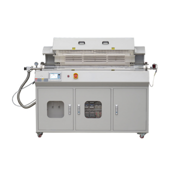
- Chemical Vapor Deposition CVD Equipment System Chamber Slide PECVD Tube Furnace with Liquid Gasifier PECVD Machine
- Inclined Rotary Plasma Enhanced Chemical Vapor Deposition PECVD Equipment Tube Furnace Machine
- RF PECVD System Radio Frequency Plasma-Enhanced Chemical Vapor Deposition RF PECVD
- Customer Made Versatile CVD Tube Furnace Chemical Vapor Deposition Chamber System Equipment
- Vacuum Hot Press Furnace Machine for Lamination and Heating
People Also Ask
- How is PECVD different from CVD? Unlock Low-Temperature Thin Film Deposition
- What is the difference between CVD and PECVD? Choose the Right Thin-Film Deposition Method
- What are the examples of CVD method? Discover the Versatile Applications of Chemical Vapor Deposition
- Why is PECVD better than CVD? Achieve Superior Low-Temperature Thin Film Deposition
- How are PECVD and CVD different? A Guide to Choosing the Right Thin-Film Deposition Process