In essence, CVD graphene is high-quality, single-layer graphene synthesized through a process called Chemical Vapor Deposition. This "bottom-up" method uses a carbon-containing gas and a metal catalyst at high temperatures to "grow" large, continuous sheets of graphene, atom by atom. It has become the most promising and widely used technique for producing the kind of large-area graphene required for electronics and industrial applications.
Chemical Vapor Deposition (CVD) solves graphene's biggest production challenge: scalability. While other methods often create small flakes, CVD is the definitive process for manufacturing uniform, single-atom-thick sheets over large areas, making it the cornerstone of advanced material and electronics development.
How the CVD Process Works: A Step-by-Step Breakdown
CVD is a highly controlled process of atomic self-assembly. Understanding its core stages reveals why it can produce such high-quality material.
The Core Ingredients
The process requires two primary components: a catalyst substrate, which is typically a thin foil of a metal like copper (Cu) or nickel (Ni), and a carbon precursor, a hydrocarbon gas such as methane (CH4).
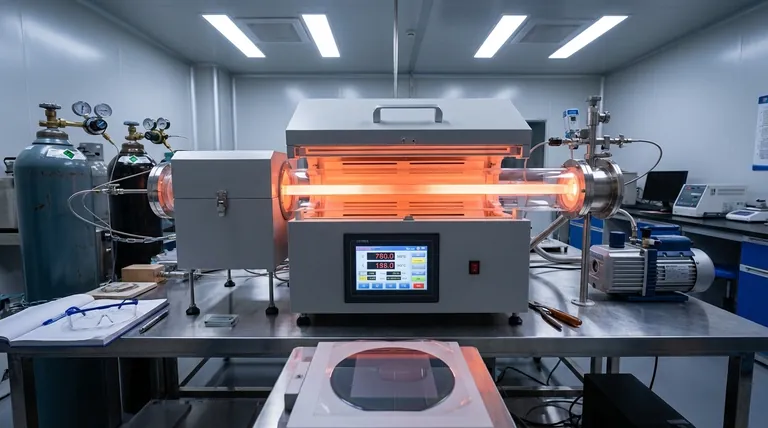
The High-Temperature Reaction
The metal foil is placed inside a furnace and heated to extreme temperatures, often around 1000 °C. Once the temperature is stable, the carbon precursor gas is introduced into the chamber.
Atomic-Level Assembly
At this high temperature, the hydrocarbon gas molecules decompose. This frees carbon atoms, which then adsorb (or bind) to the surface of the hot metal catalyst.
These carbon atoms diffuse across the metal surface, eventually nucleating and self-assembling into the stable, hexagonal lattice structure of graphene. This growth continues until a continuous, single-atom-thick film covers the substrate.
The Transfer Process
Because the graphene grows on a metal foil, a critical final step is required. The newly formed graphene sheet must be carefully transferred from the metal catalyst onto a target substrate, such as a silicon wafer or flexible polymer, for its final application.
Why CVD Is the Leading Method for Graphene Production
CVD is not just one method among many; it has emerged as the most important for practical applications due to several key advantages.
Unmatched Scalability
The primary advantage of CVD is its ability to produce large-area graphene films. This makes it suitable for industrial-scale manufacturing, including continuous roll-to-roll (R2R) production, which is impossible with methods that only yield small flakes.
High Quality and Purity
The CVD process results in graphene that is exceptionally pure and uniform. It reliably produces single-layer sheets, a critical requirement for high-performance electronics, sensors, and transparent conductive films where material consistency is paramount.
Precise Control
Engineers can precisely control the final material properties. By adjusting parameters like gas flow rate, temperature, and exposure time, it is possible to control the number of graphene layers grown on the substrate.
Understanding the Trade-offs and Challenges
Despite its advantages, CVD graphene is not without its complexities. Objectivity requires acknowledging the technical hurdles that remain.
The Complexity of Transfer
The process of transferring the fragile, one-atom-thick graphene sheet from the metal foil to the final substrate is extremely delicate. This step can introduce wrinkles, tears, and defects, which can degrade the material's exceptional electrical and mechanical properties.
The Problem of Grain Boundaries
CVD graphene growth starts at multiple points (nucleation sites) on the catalyst surface simultaneously. As these individual "islands" of graphene grow and merge, they form grain boundaries. These boundaries are imperfections in the crystal lattice that can impede electron flow and reduce overall performance.
High Energy Costs
The process relies on furnaces operating at approximately 1000 °C. Maintaining these temperatures on an industrial scale is energy-intensive, contributing significantly to the overall cost of production.
Making the Right Choice for Your Goal
Selecting the right type of graphene depends entirely on your application's specific requirements for quality, scale, and cost.
- If your primary focus is high-performance electronics or transparent conductors: CVD graphene is the ideal choice due to its high purity, large area, and single-layer uniformity.
- If your primary focus is bulk composites or conductive inks: Graphene produced by other methods, like liquid-phase exfoliation, may be more cost-effective as you need quantity (flakes) rather than a perfect, large sheet.
- If your primary focus is fundamental research: The precise control offered by CVD allows for studying the intrinsic properties of graphene, such as the effects of layer number and twist angles.
Ultimately, understanding the CVD process is key to unlocking graphene's potential to revolutionize next-generation materials and technologies.
Summary Table:
| Feature | CVD Graphene |
|---|---|
| Primary Advantage | Scalable production of large-area, uniform films |
| Key Quality | High-purity, single-layer sheets |
| Main Challenge | Delicate transfer process & grain boundaries |
| Best For | Electronics, sensors, transparent conductors |
| Not Ideal For | Low-cost bulk composites where flakes suffice |
Ready to integrate high-quality CVD graphene into your research or product development? KINTEK specializes in providing the advanced lab equipment and consumables necessary for cutting-edge material science. Our expertise supports the precise thermal processing and controlled environments required for successful CVD applications. Contact our experts today via our contact form to discuss how we can help you achieve your material synthesis goals.
Visual Guide

Related Products
- Carbon Graphite Plate Manufactured by Isostatic Pressing Method
- CVD Diamond for Thermal Management Applications
- Laboratory CVD Boron Doped Diamond Materials
- Custom CVD Diamond Coating for Lab Applications
- Vertical High Temperature Graphite Vacuum Graphitization Furnace
People Also Ask
- What is the process of isostatic graphite manufacturing? Achieve Unmatched Material Uniformity and Performance
- Why Use an Isostatic or High-Precision Hydraulic Press for Li/LLZO/Li Batteries? Master Solid-State Interfaces
- What is isostatic pressing? Achieve Uniform Density and Complex Shapes
- What is the difference between CIP and HIP? A Guide to Choosing the Right Process
- How big is the isostatic pressing market? A Deep Dive into the $1.2B+ Advanced Manufacturing Enabler