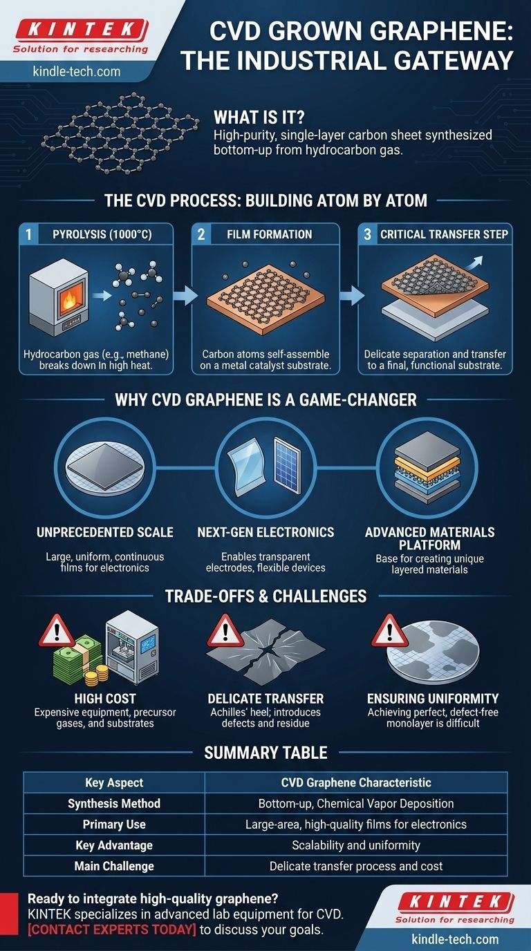
At its core, CVD grown graphene is a high-purity, single-layer sheet of carbon atoms synthesized through a process called Chemical Vapor Deposition (CVD). This "bottom-up" method involves heating a hydrocarbon gas, like methane, inside a furnace, which causes it to decompose and deposit carbon atoms onto a metal substrate, typically copper foil. These atoms then self-assemble into a large, continuous, and highly uniform graphene film.
While graphene holds immense promise, producing it at scale with consistent quality has been a central challenge. CVD is the leading industrial method for creating large-area, high-quality graphene films, making it the critical gateway for its use in next-generation electronics and advanced materials.
The CVD Process: Building Graphene Atom by Atom
The CVD method is a precision-engineering approach to material synthesis. It allows for a level of control that is difficult to achieve with other methods, building the material layer literally one atom at a time.
The Principle of Deposition
CVD is a "bottom-up" synthesis technique. Instead of starting with a large piece of graphite and stripping away layers ("top-down"), CVD builds the graphene sheet from individual carbon atoms supplied by a precursor gas.
The Two-Step Mechanism
The process unfolds in two key stages inside a high-temperature furnace, often around 1000°C.
First is pyrolysis, where the precursor hydrocarbon gas is broken down by the intense heat. This frees individual carbon atoms from their molecular bonds.
Second is film formation, where these free carbon atoms diffuse onto the surface of a metal catalyst substrate. The metal surface guides the atoms to arrange themselves into the hexagonal honeycomb lattice structure of graphene.
The Critical Transfer Step
After the graphene film has grown on the metal foil, it is not yet ready for use. The single-atom-thick sheet must be carefully separated from the metal and transferred onto a final, functional substrate, such as a silicon wafer or flexible polymer. This step is delicate and crucial to the final quality.
Why CVD Graphene Is a Game-Changer
The properties of CVD graphene make it uniquely suited for applications where both scale and performance are non-negotiable. Its value lies in its ability to bridge the gap between laboratory discovery and industrial reality.
Unprecedented Scale and Quality
CVD is the only widely used method capable of producing continuous, monolayer graphene sheets on a large scale (e.g., wafer-scale). This ability to create large, uniform films is essential for manufacturing electronic devices.
Enabling Next-Generation Electronics
CVD graphene's combination of transparency, conductivity, and flexibility makes it a prime candidate to replace existing materials. It is foundational for developing transparent electrodes for touch screens, flexible solar cells, and high-speed photodetectors.
A Platform for Advanced Materials
The high quality of CVD graphene makes it the ideal base for creating "heterostructures." These are layered stacks of different 2D materials, which can be engineered to have unique electronic or optical properties not found in any single material.
Understanding the Trade-offs and Challenges
While CVD is a powerful technique, its practical implementation comes with significant engineering hurdles. Understanding these limitations is key to appreciating its current and future applications.
The Cost Factor
The CVD process requires expensive equipment, including high-temperature vacuum furnaces and precision gas flow controllers. This, combined with the cost of high-purity precursor gases and substrates, makes it a costly method for mass production.
The Challenge of Transfer
The transfer process is the Achilles' heel of CVD graphene production. Moving the fragile, one-atom-thick film can introduce wrinkles, tears, polymer residue, and other defects that degrade its electrical and mechanical properties, impacting final device performance.
Ensuring Perfect Uniformity
While CVD produces highly uniform films, achieving a perfect, defect-free monolayer across an entire large-area wafer remains a significant engineering challenge. Small variations in growth conditions can lead to multilayer patches or grain boundaries that affect performance.
Making the Right Choice for Your Goal
The utility of CVD graphene depends entirely on your application's specific requirements for quality, scale, and cost.
- If your primary focus is fundamental research or creating novel heterostructures: CVD provides the highest-quality, large-area platform available for exploring the physics of 2D materials.
- If your primary focus is developing next-generation optoelectronics: CVD graphene is the leading candidate to replace brittle and expensive transparent conductors in devices like flexible displays and solar cells.
- If your primary focus is large-scale industrial composites or coatings: The current cost and transfer complexity of CVD may be prohibitive, but its potential to add strength without weight keeps it a key material for future aerospace and construction applications.
Ultimately, understanding the CVD process is essential for anyone looking to move graphene from a laboratory marvel to a foundational industrial material.
Summary Table:
| Key Aspect | CVD Graphene Characteristic |
|---|---|
| Synthesis Method | Bottom-up, chemical vapor deposition |
| Primary Use | Large-area, high-quality films for electronics |
| Key Advantage | Scalability and uniformity |
| Main Challenge | Delicate transfer process and cost |
Ready to integrate high-quality graphene into your research or product development?
KINTEK specializes in providing the advanced lab equipment and consumables necessary for cutting-edge material synthesis like CVD. Whether you are exploring next-generation electronics or developing novel heterostructures, our expertise can support your innovation.
Contact our experts today to discuss how we can help you achieve your materials science goals.
Visual Guide
Related Products
- Carbon Graphite Plate Manufactured by Isostatic Pressing Method
- CVD Diamond for Thermal Management Applications
- Laboratory CVD Boron Doped Diamond Materials
- Custom CVD Diamond Coating for Lab Applications
- Vertical High Temperature Graphite Vacuum Graphitization Furnace
People Also Ask
- What is isostatic graphite? The Ultimate Material for High-Tech and High-Temperature Applications
- What is isostatic pressing? Achieve Uniform Density and Complex Shapes
- What is the process of isostatic graphite manufacturing? Achieve Unmatched Material Uniformity and Performance
- What products are made by isostatic pressing? Achieve Flawless, High-Performance Components
- How is isostatic pressing distinguished from conventional pressing? Unlock Superior Uniformity and Density