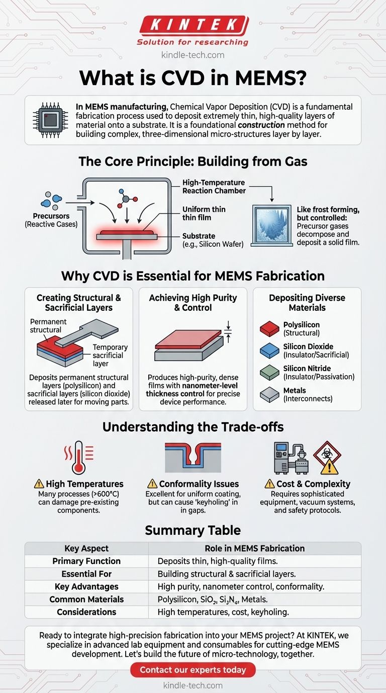
In the context of MEMS manufacturing, Chemical Vapor Deposition (CVD) is a fundamental fabrication process used to deposit extremely thin, high-quality layers of material onto a substrate. It is a primary method for building up the structural and functional layers that form the microscopic mechanical and electronic components of a Micro-Electro-Mechanical Systems (MEMS) device.
CVD is not just a coating technique; in MEMS, it is a foundational construction method. It allows engineers to build complex, three-dimensional micro-structures layer by layer from gaseous chemical precursors, enabling the creation of everything from accelerometers to micro-mirrors.
The Core Principle: Building from Gas
How CVD Works
At its core, the CVD process involves introducing reactive gases, known as precursors, into a high-temperature reaction chamber containing the substrate (typically a silicon wafer).
The heat provides the energy needed to trigger a chemical reaction. This reaction causes the precursors to decompose and deposit a solid, thin film onto the surface of the substrate.
Think of it like frost forming on a cold window pane. In that analogy, water vapor is the precursor, and the cold glass surface triggers its change from a gas to a solid. CVD is a far more controlled version of this, using specific gases to create precise, engineered solid layers.
Why CVD is Essential for MEMS Fabrication
Creating Structural and Sacrificial Layers
MEMS devices are defined by their moving parts. CVD is critical for depositing both the permanent structural layers (often polysilicon) that form the device's cantilevers, gears, or membranes.
Crucially, it is also used to deposit sacrificial layers (often silicon dioxide). These layers act as temporary placeholders that are later chemically etched away, "releasing" the structural components and allowing them to move freely.
Achieving High Purity and Control
The chemical reactions in CVD produce films of exceptionally high purity and density, which is vital for the reliable mechanical and electrical performance of a micro-device.
Furthermore, the process allows for nanometer-level control over the thickness of the deposited film. This precision is non-negotiable, as even tiny variations can drastically alter a MEMS device's resonant frequency or sensitivity.
Depositing Diverse Materials
CVD is a versatile technique capable of depositing a wide range of materials essential for MEMS. These include:
- Polysilicon: The most common structural material.
- Silicon Dioxide: Used as an electrical insulator and a sacrificial layer.
- Silicon Nitride: Used for electrical insulation and as a hard, protective passivation layer.
- Metals: Such as tungsten, for creating electrical interconnects.
Understanding the Trade-offs
The Challenge of High Temperatures
Many common CVD processes, like Low-Pressure CVD (LPCVD), require very high temperatures (often >600°C). This thermal budget can damage or alter components that have already been fabricated on the wafer, restricting the order of process steps.
Newer variants like Plasma-Enhanced CVD (PECVD) operate at lower temperatures but sometimes at the cost of film quality.
Conformality: A Double-Edged Sword
CVD is known for its excellent conformality, meaning it coats all surfaces of a three-dimensional feature evenly, including vertical sidewalls and deep trenches.
This is a huge advantage for creating uniform structural layers. However, it can be a disadvantage when the goal is to fill a gap or trench without creating a void, a challenge known as "keyholing."
Cost and Complexity
CVD reactors are sophisticated and expensive pieces of equipment. They require vacuum systems, precise temperature and gas flow control, and infrastructure to handle potentially hazardous precursor gases, making the process a significant capital investment.
How to Apply This to Your Project
Understanding the role of CVD helps clarify its importance relative to other fabrication steps. When designing a MEMS fabrication flow, consider how CVD fits your specific goal.
- If your primary focus is creating moving parts: CVD is indispensable for depositing both the structural material and the sacrificial layers that are removed to release those parts.
- If your primary focus is electrical isolation or passivation: CVD is the industry standard for depositing high-quality, dense insulating films like silicon dioxide and silicon nitride.
- If your primary focus is precise thickness control: CVD offers superior control over film thickness compared to many other deposition techniques, which is critical for predictable device performance.
Ultimately, mastering CVD is fundamental to mastering the art of building functional machines at the micro-scale.
Summary Table:
| Key Aspect | Role in MEMS Fabrication |
|---|---|
| Primary Function | Deposits thin, high-quality films of material onto a substrate. |
| Essential For | Building structural layers (e.g., polysilicon) and sacrificial layers (e.g., silicon dioxide). |
| Key Advantages | High film purity, nanometer-level thickness control, excellent conformal coating. |
| Common Materials | Polysilicon, Silicon Dioxide (SiO₂), Silicon Nitride (Si₃N₄), Metals (e.g., Tungsten). |
| Considerations | High process temperatures, equipment cost and complexity, potential for keyholing. |
Ready to integrate high-precision fabrication into your MEMS project?
At KINTEK, we specialize in providing the advanced lab equipment and consumables necessary for cutting-edge MEMS development. Whether you are depositing structural polysilicon or insulating silicon nitride, our solutions help you achieve the nanometer-level control and material purity your designs demand.
Let's build the future of micro-technology, together. Contact our experts today to discuss how we can support your specific fabrication challenges.
Visual Guide
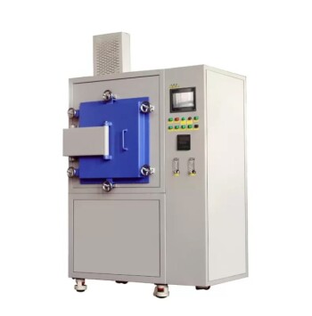
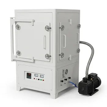
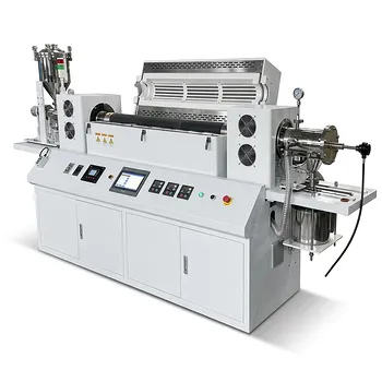
Related Products
- Customer Made Versatile CVD Tube Furnace Chemical Vapor Deposition Chamber System Equipment
- Multi Heating Zones CVD Tube Furnace Machine Chemical Vapor Deposition Chamber System Equipment
- Horizontal High Temperature Graphite Vacuum Graphitization Furnace
- Controlled Nitrogen Inert Hydrogen Atmosphere Furnace
- Vertical High Temperature Graphite Vacuum Graphitization Furnace
People Also Ask
- What is a CVD tube furnace? A Complete Guide to Thin-Film Deposition
- What is the temperature of a CVD furnace? From 200°C to 1600°C for Precise Film Deposition
- What is the function of a high-temperature CVD tube furnace in 3D graphene foam prep? Master 3D Nanomaterial Growth
- What is the synthesis and mechanism involved in the preparation of carbon nanotubes using CVD process? Master Controlled Growth for Your Application
- What is a CVD furnace? The Ultimate Guide to Precision Thin-Film Coating