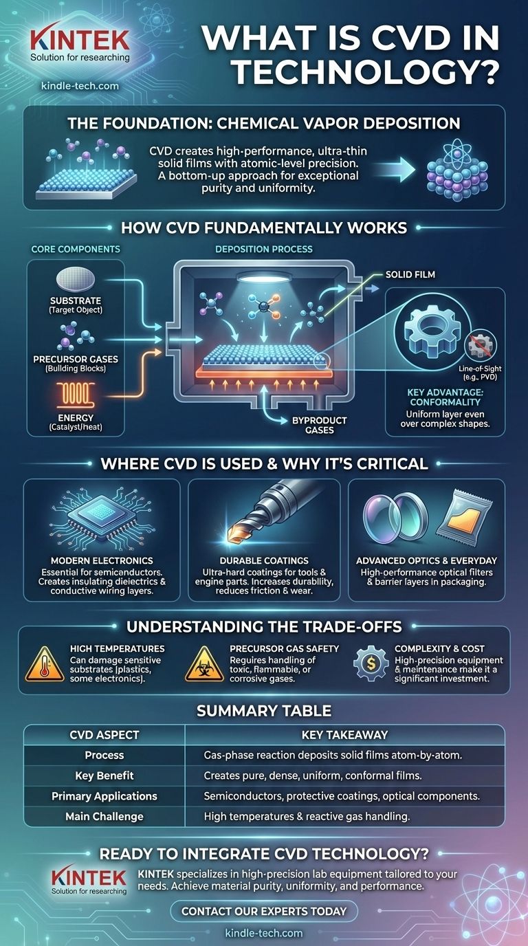
In technology, CVD, or Chemical Vapor Deposition, is a foundational manufacturing process used to create high-performance, ultra-thin solid films. It works by introducing reactive gases into a chamber, which then decompose and form a solid material layer directly onto a target object, or substrate. This method is the backbone for building materials with atomic-level precision, enabling everything from advanced microchips to durable coatings on industrial tools.
The core value of CVD lies in its ability to construct materials from the ground up, atom by atom. This bottom-up approach allows for the creation of films that are exceptionally pure, dense, and uniform, enabling performance characteristics unattainable through traditional manufacturing methods.
How CVD Fundamentally Works
At its heart, CVD is a sophisticated chemical process that turns gas into a solid. Imagine it not as spraying a pre-made paint, but as releasing two invisible gases that only react and form solid paint particles at the precise moment they hit the target surface.
The Core Components
Every CVD process involves three key elements:
- Substrate: This is the object to be coated. It can be a silicon wafer for a computer chip, a medical implant, or a machine tool.
- Precursor Gases: These are the gaseous "building block" molecules. They contain the atoms (e.g., silicon, tungsten, carbon) needed to form the final solid film.
- Energy: Usually in the form of high heat, this energy is applied to the substrate. It acts as the catalyst, breaking down the precursor gases and initiating the chemical reaction.
The Deposition Process
The substrate is placed inside a vacuum chamber and heated to a specific temperature. Precursor gases are then carefully introduced into the chamber. The intense heat causes these gas molecules to react and decompose near the substrate's surface.
The desired atoms from the gas then bond with the substrate, forming a thin, solid, and highly adherent film. Unwanted byproduct gases from the reaction are simply pumped out of the chamber, leaving behind an exceptionally pure layer of the new material.
Why This Method is Powerful
The power of CVD comes from its precision control. Because the film is literally built atom by atom, the resulting layer is incredibly uniform, even over complex, three-dimensional shapes. This is known as conformality, and it is a critical advantage over line-of-sight methods like physical sputtering or simple plating.
Where CVD is Used and Why it is Critical
CVD is not a single technique but a family of processes that have become indispensable across numerous high-tech industries. Its ability to create materials with specific, engineered properties makes it a versatile and vital tool.
The Foundation of Modern Electronics
The semiconductor industry would not exist in its current form without CVD. It is used to deposit the critical layers that make up transistors, the microscopic on-off switches at the heart of every microchip. This includes depositing insulating layers (dielectrics) to prevent electrical leakage and conductive layers to form the "wires" connecting millions of transistors.
Creating Durable and Protective Coatings
In heavy industry and aerospace, CVD is used to apply ultra-hard coatings to cutting tools, drill bits, and engine components. These coatings, often made of materials like titanium nitride or diamond-like carbon, drastically increase durability, reduce friction, and provide resistance to wear and corrosion.
Advanced Optics and Everyday Materials
CVD is essential for manufacturing high-performance optical components. It is used to apply anti-reflective coatings on lenses and to create specialized optical filters. In a more common application, a similar vapor deposition process is used to apply the microscopically thin layer of aluminum inside potato chip bags, creating a barrier against oxygen and moisture.
Understanding the Trade-offs of CVD
While incredibly powerful, CVD is not a universal solution. Its implementation involves significant technical challenges and trade-offs that are important to understand.
The Need for High Temperatures
Traditional CVD often requires very high temperatures (several hundred to over a thousand degrees Celsius). This intense heat can damage or warp temperature-sensitive substrates, such as plastics or electronic devices with pre-existing low-melting-point materials.
Precursor Gas Handling and Safety
The precursor gases used in CVD are often highly toxic, flammable, or corrosive. Managing these materials requires complex and expensive safety protocols, specialized storage, and sophisticated delivery systems, which adds significantly to the operational cost and complexity.
Process Complexity and Cost
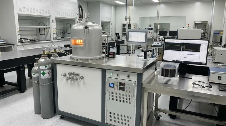
CVD systems are precision machines. The need for vacuum chambers, high-temperature heating elements, and precise gas flow control makes the equipment expensive to purchase and maintain. It is a high-cost, high-precision process reserved for applications where the performance benefits justify the investment.
Making the Right Choice for Your Goal
Understanding CVD is about recognizing its role as a high-precision tool for creating materials with superior properties. How you apply this knowledge depends on your field.
- If your primary focus is electronics and semiconductors: CVD is the fundamental process enabling Moore's Law, allowing the fabrication of smaller, faster, and more powerful integrated circuits.
- If your primary focus is materials science and engineering: CVD is a key method for surface engineering, used to create materials with enhanced properties like extreme hardness, chemical inertness, or specific electrical conductivity.
- If your primary focus is general manufacturing: View CVD as an advanced coating technology used when standard painting or plating cannot deliver the required uniformity, purity, or performance.
Ultimately, Chemical Vapor Deposition is the invisible engineering that transforms gases into the high-performance solid materials that define our modern technological world.
Summary Table:
| CVD Aspect | Key Takeaway |
|---|---|
| Process | Gas-phase chemical reaction deposits solid films atom-by-atomic layer onto a substrate. |
| Key Benefit | Creates exceptionally pure, dense, and uniform films with superior conformality over complex shapes. |
| Primary Applications | Semiconductor manufacturing, ultra-hard protective coatings, advanced optical components. |
| Main Challenge | High process temperatures and handling of reactive/toxic precursor gases. |
Ready to Integrate CVD Technology into Your Lab?
CVD is the cornerstone of modern high-performance materials. Whether you are developing next-generation semiconductors, creating durable coatings for industrial tools, or engineering advanced optical components, having the right equipment is critical.
KINTEK specializes in providing high-precision lab equipment and consumables tailored to your research and production needs. Our expertise can help you select the right CVD solutions to achieve the material purity, uniformity, and performance your projects demand.
Contact our experts today to discuss how we can support your laboratory's specific challenges and goals with reliable, cutting-edge technology.
Visual Guide
Related Products
- CVD Diamond Dressing Tools for Precision Applications
- Multi Heating Zones CVD Tube Furnace Machine Chemical Vapor Deposition Chamber System Equipment
- CVD Diamond Domes for Industrial and Scientific Applications
- CVD Diamond for Thermal Management Applications
- Chemical Vapor Deposition CVD Equipment System Chamber Slide PECVD Tube Furnace with Liquid Gasifier PECVD Machine
People Also Ask
- How long does it take to make synthetic diamonds? Discover the 6-8 Week Science Behind Lab-Grown Gems
- What are the raw materials for CVD diamonds? A seed, a gas, and the science of crystal growth.
- What are the disadvantages of CVD diamonds? Understanding the trade-offs for your purchase.
- How do CVD diamonds grow? A Step-by-Step Guide to Lab-Grown Diamond Creation
- How do you identify a CVD diamond? The Definitive Guide to Lab-Grown Diamond Verification


