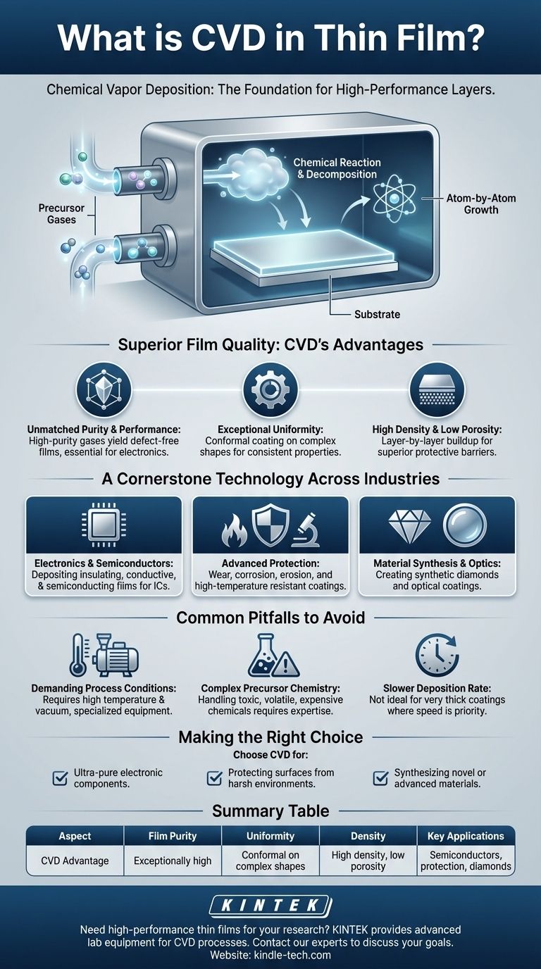
In the context of thin films, Chemical Vapor Deposition (CVD) is a highly versatile manufacturing process used to create exceptionally pure and high-performance solid layers on a substrate. It works by introducing precursor gases into a chamber, which then react or decompose on the surface of the object to be coated, building the desired thin film atom by atom. This method is fundamental to producing materials with superior quality, uniformity, and low porosity.
The critical takeaway is that CVD is not just another coating technique; it is a foundational process for engineering materials at the atomic level. Its value lies in its ability to produce films with unparalleled purity and structural integrity, making it indispensable for the most demanding applications, from microchips to protective coatings.
How CVD Achieves Superior Film Quality
CVD's unique approach of building a film from gaseous precursors is the source of its primary advantages. The process allows for an exceptional degree of control over the final material's properties.
Unmatched Purity and Performance
The precursors are high-purity gases, which translates directly into a high-purity solid film. This is non-negotiable in industries like semiconductor manufacturing, where even trace impurities can render a microchip useless.
Exceptional Uniformity
Because the film is deposited from a vapor phase, it can conformally coat complex shapes and surfaces. This ensures the resulting layer has a consistent thickness and properties across the entire object, which is vital for performance.
High Density and Low Porosity
The CVD process builds films layer by layer, resulting in a dense, solid material with very few pores or defects. This characteristic is the reason CVD coatings create such effective protective barriers.
A Cornerstone Technology Across Industries
The high-quality films produced by CVD are essential in a wide range of fields. The applications are diverse, but they are all unified by a need for high performance and reliability.
In Electronics and Semiconductors
CVD is a workhorse in the semiconductor industry. It is used to deposit the various thin films—insulating, conductive, and semiconducting—that form the intricate structures of integrated circuits and microprocessors.
For Advanced Protection
The dense nature of CVD films makes them ideal for creating protective barriers. They are used to make components resistant to wear, corrosion, erosion, and high temperatures, extending the life and reliability of critical parts.
In Material Synthesis and Optics
CVD is powerful enough to create entirely new materials. Its most famous application in this area is the synthesis of high-quality diamonds for industrial tools and even jewelry. It is also used to create optical coatings and gas-tight barrier layers on glass and plastic.
Common Pitfalls to Avoid
While powerful, the precision of CVD comes with inherent complexities. Understanding these is key to leveraging the technology effectively.
Demanding Process Conditions
CVD often requires high temperatures and vacuum conditions to facilitate the necessary chemical reactions. This requires specialized, and often costly, equipment and significant energy consumption.
Precursor Chemistry is Complex
The choice and handling of precursor gases are critical. These chemicals can be toxic, volatile, or expensive, and managing the reaction chemistry to achieve the desired film properties requires deep process expertise.
Deposition Rate Can Be a Limiter
Compared to some physical deposition methods, CVD can have a slower deposition rate. For applications requiring very thick coatings where ultimate purity is not the primary concern, other methods may be more economical.
Making the Right Choice for Your Goal
Selecting CVD is a decision based on the required performance of the final thin film.
- If your primary focus is creating ultra-pure electronic components: CVD is the industry standard for depositing the high-performance, defect-free thin films required for modern semiconductors.
- If your primary focus is protecting surfaces from harsh environments: CVD provides dense, non-porous coatings that offer superior and reliable resistance to corrosion, wear, and high temperatures.
- If your primary focus is synthesizing novel or advanced materials: CVD offers a precise, bottom-up method for building materials like synthetic diamonds and specialized optical layers.
Ultimately, Chemical Vapor Deposition is the definitive choice when the performance, purity, and integrity of a thin film are paramount to your success.
Summary Table:
| Aspect | CVD Advantage |
|---|---|
| Film Purity | Exceptionally high due to pure gaseous precursors |
| Uniformity | Conformal coating on complex shapes |
| Density | High density, low porosity for superior barriers |
| Key Applications | Semiconductors, protective coatings, synthetic diamonds |
Need a high-performance thin film for your application?
KINTEK specializes in providing advanced lab equipment and consumables for precise Chemical Vapor Deposition processes. Whether you are developing next-generation semiconductors, creating wear-resistant protective coatings, or synthesizing advanced materials, our solutions deliver the purity and uniformity your research demands.
Contact our experts today to discuss how our CVD technology can enhance your laboratory's capabilities and achieve your material science goals.
Visual Guide
Related Products
- CVD Diamond Dressing Tools for Precision Applications
- Multi Heating Zones CVD Tube Furnace Machine Chemical Vapor Deposition Chamber System Equipment
- CVD Diamond Domes for Industrial and Scientific Applications
- CVD Diamond for Thermal Management Applications
- Chemical Vapor Deposition CVD Equipment System Chamber Slide PECVD Tube Furnace with Liquid Gasifier PECVD Machine
People Also Ask
- How long does it take to make synthetic diamonds? Discover the 6-8 Week Science Behind Lab-Grown Gems
- What are the disadvantages of CVD diamonds? Understanding the trade-offs for your purchase.
- How do you identify a CVD diamond? The Definitive Guide to Lab-Grown Diamond Verification
- How do CVD diamonds grow? A Step-by-Step Guide to Lab-Grown Diamond Creation
- What is CVD diamond? The Ultimate Guide to Lab-Grown Diamonds and Their Uses


