At its core, Chemical Vapor Deposition (CVD) is a highly controlled process for manufacturing a thin solid film on a surface. It works by introducing specific gases, known as precursors, into a chamber containing a heated object, or substrate. The heat triggers a chemical reaction in the gases, causing a new solid material to "grow" or deposit onto the substrate, molecule by molecule.
Chemical Vapor Deposition is not simply a coating technique; it is fundamentally a chemical synthesis process performed at an atomic scale. The key is using heat to trigger a precise gas-phase reaction that builds a solid material directly onto a target surface.
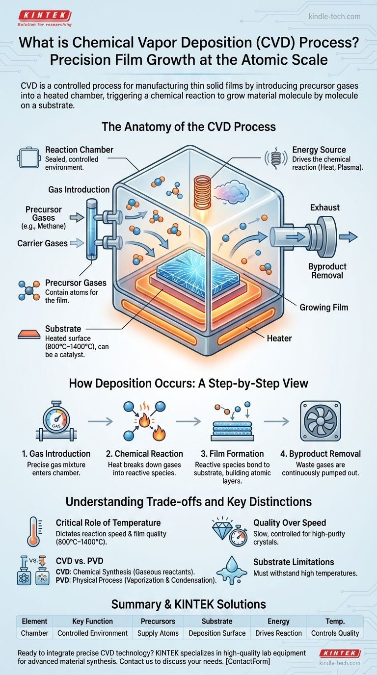
The Anatomy of the CVD Process
To understand how CVD works, it's best to break it down into its essential components. Each element plays a critical role in the final quality and composition of the deposited film.
The Reaction Chamber
This is the sealed, controlled environment where the entire process takes place. It allows for the precise management of pressure, gas composition, and the removal of unwanted byproducts.
The Precursor Gases
These are the gaseous "ingredients" that contain the atoms of the material you want to deposit. For example, to grow a diamond film, the chamber would be filled with carbon-containing gases like methane. These are often mixed with inert carrier gases to control their concentration and flow.
The Substrate
This is the object or surface onto which the film is deposited. The substrate is heated to very high temperatures, often between 800°C and 1400°C, providing the energy needed to initiate the chemical reaction. In many cases, the substrate is not just a passive surface; it can act as a catalyst, actively promoting and guiding the reaction.
The Energy Source
Heat is the primary driver of the CVD process. This energy is delivered using methods like hot filaments, lasers, or microwave induction. In some advanced CVD methods, an RF plasma is also used to help break down the precursor gases into more reactive forms at lower temperatures.
How Deposition Occurs: A Step-by-Step View
The elegance of CVD lies in its carefully orchestrated sequence of events, transforming gas into a solid.
Step 1: Gas Introduction
A precise mixture of precursor and carrier gases is directed into the reaction chamber at a controlled flow rate.
Step 2: Chemical Reaction
As the gases come into contact with or pass near the hot substrate, the intense heat breaks them down. This dissociation creates highly reactive atoms and molecules that are now ready to form a new material.
Step 3: Film Formation
These reactive chemical species diffuse toward the cooler substrate. Upon reaching the surface, they undergo further chemical reactions, bonding together and to the substrate itself. This is an atomistic process that builds a solid film one atomic layer at a time.
Step 4: Byproduct Removal
The chemical reactions often create waste gases as byproducts. These, along with any unreacted precursor gases, are continuously pumped out of the chamber to maintain a pure environment for deposition.
Understanding the Trade-offs and Key Distinctions
While powerful, CVD is not a universal solution. Its effectiveness depends on managing critical parameters and understanding its inherent trade-offs.
The Central Role of Temperature
Substrate temperature is the most critical variable in CVD. It dictates whether a reaction occurs, the speed of the reaction, and the final properties of the film. Too low, and deposition won't happen; too high, and you may get unwanted side reactions or a poorly structured, amorphous film instead of a perfect crystal.
CVD vs. PVD: A Crucial Distinction
It's vital to distinguish CVD from Physical Vapor Deposition (PVD). PVD is a physical process where a solid material is vaporized (by evaporation or sputtering) and then simply condenses on the substrate. CVD is a chemical process where new materials are synthesized directly on the substrate from gaseous reactants.
Quality Over Speed
Achieving a high-purity, perfectly ordered crystalline structure, such as for graphene or lab-grown diamonds, requires immense control and is often a slow process. It can take days or even weeks, and technicians may need to periodically halt the process to remove unwanted byproducts, like graphite, that can form alongside the desired material.
Substrate Limitations
The high temperatures required for many CVD processes limit the types of materials that can be used as substrates. The substrate must be able to withstand the heat without melting, deforming, or reacting undesirably with the precursor gases.
Making the Right Choice for Your Goal
Applying CVD effectively requires aligning the process variant with your specific technical objective.
- If your primary focus is creating ultra-pure, crystalline materials (like semiconductors or lab-grown diamonds): Traditional high-temperature CVD is the ideal method, as its controlled chemical reactions allow for precise, layer-by-layer growth.
- If your primary focus is applying a functional coating to a temperature-sensitive material (like a polymer): You must use a lower-temperature variant like Plasma-Enhanced CVD (PECVD) or consider a different method like PVD entirely.
- If your primary focus is a thick, durable protective coating on a robust metal part: High-temperature, high-pressure CVD can be a very effective and relatively fast choice, provided the part can tolerate the conditions.
Ultimately, mastering CVD is about precisely controlling a chemical reaction to build your desired material from the atoms up.
Summary Table:
| CVD Process Element | Key Function |
|---|---|
| Reaction Chamber | Sealed environment for precise control of pressure and gas composition |
| Precursor Gases | Supply atoms for the desired film material (e.g., methane for diamond) |
| Substrate | Heated surface where deposition occurs; can act as a catalyst |
| Energy Source | Provides heat (or plasma) to drive the chemical reaction |
| Temperature | Critical variable controlling reaction speed and film quality (800°C–1400°C) |
Ready to integrate precise CVD technology into your lab? At KINTEK, we specialize in providing high-quality lab equipment and consumables tailored for advanced material synthesis. Whether you're developing semiconductors, growing diamonds, or applying functional coatings, our expertise ensures you achieve superior film quality and process efficiency. Contact our experts today to discuss how our solutions can meet your specific laboratory needs and drive your research forward.
Visual Guide
Related Products
- CVD Diamond Dressing Tools for Precision Applications
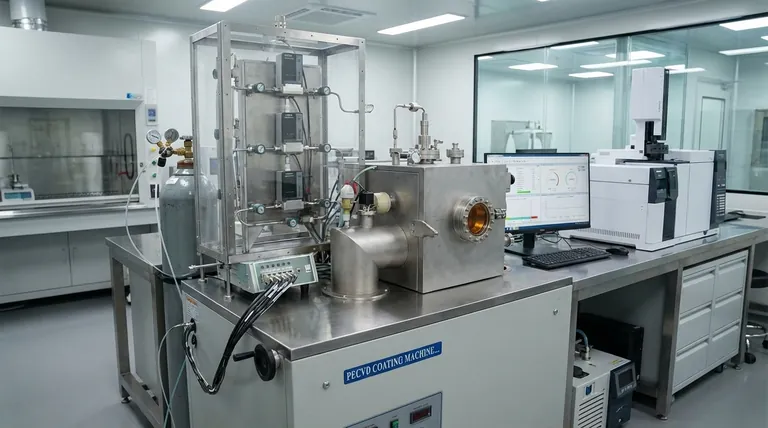
- Multi Heating Zones CVD Tube Furnace Machine Chemical Vapor Deposition Chamber System Equipment
- CVD Diamond Domes for Industrial and Scientific Applications
- CVD Diamond for Thermal Management Applications
- Chemical Vapor Deposition CVD Equipment System Chamber Slide PECVD Tube Furnace with Liquid Gasifier PECVD Machine
People Also Ask
- How long does it take to make synthetic diamonds? Discover the 6-8 Week Science Behind Lab-Grown Gems
- How do CVD diamonds grow? A Step-by-Step Guide to Lab-Grown Diamond Creation
- What is chemical vapor deposition of diamond? Grow High-Purity Diamonds Atom-by-Atom
- What are the disadvantages of CVD diamonds? Understanding the trade-offs for your purchase.
- What color diamonds are CVD? Understanding the Process from Brown Tint to Colorless Beauty


