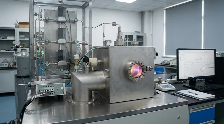
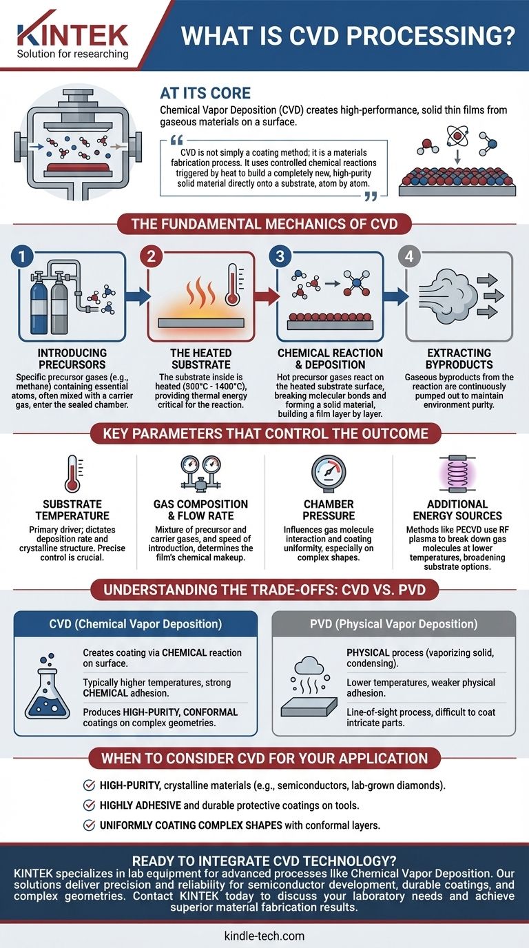
At its core, Chemical Vapor Deposition (CVD) is a sophisticated process for creating high-performance, solid thin films on a surface from gaseous materials. It involves introducing precursor gases into a reaction chamber where they interact with a heated object (the substrate), causing a chemical reaction that deposits a new, solid layer onto the object's surface.
The crucial insight is that CVD is not simply a coating method; it is a materials fabrication process. It uses controlled chemical reactions triggered by heat to build a completely new, high-purity solid material directly onto a substrate, atom by atom or molecule by molecule.
The Fundamental Mechanics of CVD
To understand CVD, it's best to break it down into its core operational steps. Each stage is precisely controlled to determine the final properties of the deposited film.
Introducing the Precursors
The process begins by introducing specific gases, known as precursors, into a sealed chamber. These gases contain the essential atoms of the film you intend to create. For example, to create a diamond film, carbon-rich gases like methane are used.
These precursors are often mixed with a carrier gas, an inert gas that helps transport the reactive molecules to the substrate at a controlled rate.
The Role of the Heated Substrate
Inside the chamber is the object to be coated, known as the substrate. This substrate is heated to a very high temperature, typically between 800°C and 1400°C.
The substrate's temperature is the most critical parameter in the entire process. It provides the necessary thermal energy to initiate the chemical reactions and can even act as a catalyst.
The Chemical Reaction and Deposition
When the hot precursor gases come into contact with the heated substrate, the energy causes their molecular bonds to break. This triggers a chemical reaction directly on or very near the substrate's surface.
The result of this reaction is the formation of a solid material that bonds to the substrate, creating a thin film. This deposition process builds up the film layer by layer, ensuring a uniform and often highly pure coating.
Extracting the Byproducts
The chemical reactions that form the solid film also create gaseous byproducts. These waste gases are continuously pumped out of the chamber to maintain the purity of the environment and allow the deposition process to continue efficiently.
Key Parameters That Control the Outcome
The quality, thickness, and structure of the film created by CVD are not accidental. They are the direct result of carefully managing several key variables.
Substrate Temperature
As the primary driver of the reaction, temperature dictates the rate of deposition and the crystalline structure of the film. A small change in temperature can significantly alter the final material's properties.
Gas Composition and Flow Rate
The specific mixture of precursor and carrier gases, along with the speed at which they are introduced, determines the chemical makeup of the film. This allows for the creation of very specific material compounds.
Chamber Pressure
The pressure inside the chamber influences how the gas molecules move and interact. It affects the uniformity of the coating, especially on complex-shaped substrates. CVD is typically considered a higher-pressure process compared to alternatives.
Additional Energy Sources
While heat is the traditional catalyst, many modern CVD processes use other energy sources to enhance the reaction. Methods like Plasma-Enhanced CVD (PECVD) use an RF plasma to break down gas molecules at lower temperatures, broadening the range of usable substrates.
Understanding the Trade-offs: CVD vs. PVD
CVD is often compared to its counterpart, Physical Vapor Deposition (PVD). Understanding their differences is key to choosing the right technology.
The Chemical vs. Physical Distinction
This is the most fundamental difference. CVD creates the coating through a chemical reaction on the substrate's surface. In contrast, PVD is a physical process that involves vaporizing a solid material and having it condense onto the substrate, like steam frosting a cold window.
Temperature and Adhesion
CVD typically requires much higher temperatures, which can limit the types of materials that can be used as substrates. However, the chemical bond formed during CVD often results in exceptionally strong and durable adhesion between the film and the substrate.
Coating Characteristics
The chemical nature of CVD allows it to produce highly pure, dense, and crystalline films. It is particularly effective at creating conformal coatings, meaning it can uniformly cover complex, non-flat surfaces. PVD is generally a line-of-sight process, which can make it difficult to coat intricate geometries.
When to Consider CVD for Your Application
Choosing the right deposition technology depends entirely on your end goal. CVD excels in specific scenarios where material purity and structural integrity are paramount.
- If your primary focus is creating high-purity, crystalline materials: CVD is the industry standard for applications like manufacturing semiconductors and lab-grown diamonds.
- If your primary focus is a highly adhesive and durable coating: The chemical bonding inherent in CVD provides superior adhesion for protective layers on tools and components.
- If your primary focus is uniformly coating complex shapes: CVD's ability to deposit a conformal layer makes it ideal for intricate parts where line-of-sight methods would fail.
Ultimately, Chemical Vapor Deposition is a foundational technology that empowers engineers and scientists to construct advanced materials from the ground up.
Summary Table:
| CVD Process Stage | Key Function | Impact on Final Film |
|---|---|---|
| Precursor Introduction | Gases containing film atoms enter the chamber. | Determines the chemical makeup of the material. |
| Substrate Heating | The substrate is heated to high temperatures (800°C-1400°C). | Drives the chemical reaction; controls deposition rate and structure. |
| Chemical Reaction & Deposition | Precursors react on the hot substrate surface. | Builds the solid film layer by layer, ensuring uniformity and purity. |
| Byproduct Extraction | Waste gases are pumped out of the chamber. | Maintains a pure environment for consistent, high-quality deposition. |
Ready to integrate CVD technology into your lab's workflow?
KINTEK specializes in providing the lab equipment and consumables you need to leverage advanced processes like Chemical Vapor Deposition. Whether you are developing semiconductors, creating durable protective coatings, or working with complex part geometries, our solutions are designed to deliver the precision and reliability your research demands.
Contact KINTEK today to discuss how we can support your specific laboratory needs and help you achieve superior material fabrication results.
Visual Guide
Related Products
- CVD Diamond Dressing Tools for Precision Applications
- Multi Heating Zones CVD Tube Furnace Machine Chemical Vapor Deposition Chamber System Equipment
- CVD Diamond Domes for Industrial and Scientific Applications
- CVD Diamond for Thermal Management Applications
- Chemical Vapor Deposition CVD Equipment System Chamber Slide PECVD Tube Furnace with Liquid Gasifier PECVD Machine
People Also Ask
- How long does it take to make synthetic diamonds? Discover the 6-8 Week Science Behind Lab-Grown Gems
- Does the chemical vapor deposition be used for diamonds? Yes, for Growing High-Purity Lab Diamonds
- What are the raw materials for CVD diamonds? A seed, a gas, and the science of crystal growth.
- Can CVD diamonds change color? No, their color is permanent and stable.
- What is CVD diamond? The Ultimate Guide to Lab-Grown Diamonds and Their Uses


