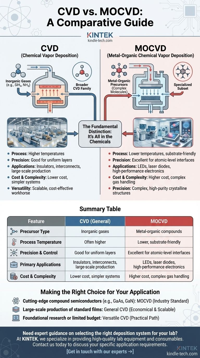
At its core, Metal-Organic Chemical Vapor Deposition (MOCVD) is a highly specialized subset of the broader Chemical Vapor Deposition (CVD) family. The primary difference lies in the chemical precursors used: MOCVD utilizes complex metal-organic compounds, while general CVD processes can use a wider variety of often simpler inorganic chemicals. This fundamental choice of precursor dictates the process conditions, film quality, and ultimate application of the technique.
While both processes deposit thin films atom-by-atom from a gas phase, the key distinction is one of precision versus versatility. MOCVD is the tool for creating complex, high-purity crystalline structures with exceptional control, whereas the broader CVD category offers a more scalable and cost-effective workhorse for a wider range of materials.
The Fundamental Distinction: It's All in the Chemicals
The "CV" in both names stands for "Chemical Vapor," which refers to the gaseous precursor chemicals that carry the desired atoms to a substrate surface. The choice of this precursor is the defining difference between MOCVD and other CVD methods.
What is a Precursor?
A precursor is a molecule that contains the element you want to deposit, but in a volatile form that can be transported as a gas or vapor. When this vapor reaches the hot substrate, the molecule breaks apart (decomposes), leaving the desired element behind as a thin film.
MOCVD's Use of Metal-Organics
MOCVD uses metal-organic precursors, which are complex molecules where a metal atom is bonded to organic (carbon-based) ligands.
These sophisticated chemicals are often liquids or solids that can be vaporized at low temperatures. This allows the entire deposition process to run at a lower temperature compared to many other CVD techniques.
General CVD's Broader Precursor Range
The general CVD category encompasses numerous techniques that can use a wider array of precursors, most commonly simple inorganic gases.
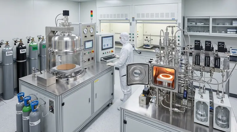
For example, depositing silicon nitride might use silane (SiH₄) and ammonia (NH₃) gas. These processes are often simpler and use more readily available, less expensive chemicals.
How Precursors Dictate Process and Performance
The difference in chemical starting materials leads to significant divergences in process capability, precision, and the quality of the final film.
The Advantage of Lower Temperatures in MOCVD
Because metal-organic precursors decompose at relatively low temperatures, MOCVD is ideal for depositing films on substrates that cannot withstand high heat. This is a critical advantage for fabricating complex, multi-layered semiconductor devices.
Unmatched Precision and Film Quality
MOCVD provides an exceptionally high degree of control. It allows for the growth of high-purity, single-crystal films and the creation of abrupt interfaces—perfectly sharp transitions between different material layers—which is essential for high-performance electronics and optoelectronics like LEDs and laser diodes.
This process also enables precise dopant control, allowing engineers to meticulously introduce impurities to tune a material's electrical properties.
The Versatility and Scalability of General CVD
While less precise than MOCVD, various CVD techniques are the backbone of the semiconductor industry for a reason. They are highly reliable, well-understood, and can be scaled up for massive industrial production of simpler, uniform films like silicon dioxide (insulators) or tungsten (interconnects).
Understanding the Trade-offs: Cost vs. Capability
Choosing between MOCVD and another CVD process is a classic engineering trade-off between performance requirements and economic reality. There is no single "better" technique; there is only the right tool for the job.
The Higher Cost and Complexity of MOCVD
MOCVD systems are complex and expensive. The metal-organic precursors themselves are costly to synthesize and purify, and the reactors require sophisticated gas handling and safety systems, making it a high-investment technology.
The Simplicity and Cost-Effectiveness of CVD
Many general CVD systems are significantly cheaper and simpler to operate and maintain. For applications where atomic-level perfection is not required, they provide an excellent balance of quality, throughput, and cost, making them practical for both large-scale production and budget-conscious research labs.
The Application Determines the Choice
A university lab might use a simple, low-cost CVD system for foundational material science research. A high-volume memory chip factory will use highly optimized, large-scale CVD systems. A company fabricating cutting-edge laser diodes or high-frequency transistors will invest in MOCVD for its unparalleled precision.
Making the Right Choice for Your Application
Your final decision must be guided by the specific requirements of the film you need to create and the device you intend to build.
- If your primary focus is on cutting-edge compound semiconductors (e.g., GaAs, GaN, InP for LEDs, lasers, or high-power transistors): MOCVD is the industry standard due to its precision and ability to grow high-quality crystalline films.
- If your primary focus is on large-scale production of standard films (e.g., silicon dioxide, silicon nitride, polysilicon, or tungsten): A specific, optimized form of general CVD (like LPCVD or PECVD) is almost always the more economical and scalable choice.
- If your primary focus is on foundational research or applications with a limited budget: A versatile, simpler CVD system often provides the most practical path forward, avoiding the high cost and complexity of MOCVD.
Ultimately, understanding this distinction empowers you to select the deposition technique that aligns perfectly with your technical goals and economic constraints.
Summary Table:
| Feature | CVD (General) | MOCVD |
|---|---|---|
| Precursor Type | Inorganic gases (e.g., SiH₄, NH₃) | Metal-organic compounds |
| Process Temperature | Often higher | Lower, substrate-friendly |
| Precision & Control | Good for uniform layers | Excellent for atomic-level interfaces |
| Primary Applications | Insulators, interconnects, large-scale production | LEDs, laser diodes, high-performance electronics |
| Cost & Complexity | Lower cost, simpler systems | Higher cost, complex gas handling |
Need expert guidance on selecting the right deposition system for your lab?
At KINTEK, we specialize in providing high-quality lab equipment and consumables tailored to your research and production needs. Whether you're working on large-scale semiconductor production or cutting-edge optoelectronics, our team can help you choose between versatile CVD systems or precision MOCVD reactors to optimize your thin-film processes.
Contact us today to discuss your specific application requirements and discover how our solutions can enhance your laboratory's capabilities.
Get in touch with our experts →
Visual Guide
Related Products
- CVD Diamond Dressing Tools for Precision Applications
- Multi Heating Zones CVD Tube Furnace Machine Chemical Vapor Deposition Chamber System Equipment
- CVD Diamond Domes for Industrial and Scientific Applications
- CVD Diamond for Thermal Management Applications
- Chemical Vapor Deposition CVD Equipment System Chamber Slide PECVD Tube Furnace with Liquid Gasifier PECVD Machine
People Also Ask
- Does the chemical vapor deposition be used for diamonds? Yes, for Growing High-Purity Lab Diamonds
- What are the raw materials for CVD diamonds? A seed, a gas, and the science of crystal growth.
- What are the disadvantages of CVD diamonds? Understanding the trade-offs for your purchase.
- How long does it take to make synthetic diamonds? Discover the 6-8 Week Science Behind Lab-Grown Gems
- How do you identify a CVD diamond? The Definitive Guide to Lab-Grown Diamond Verification


