In short, electron beam (e-beam) evaporation is a high-precision process used to create exceptionally pure, thin films on a surface. It works by using a focused, high-energy beam of electrons to vaporize a source material inside a vacuum chamber. This vapor then travels and condenses onto a target object, known as a substrate, forming a uniform coating.
E-beam evaporation is fundamentally a method of converting a solid material directly into a high-purity vapor using an intense electron beam. This allows for the precise deposition of thin films from materials that are otherwise difficult to vaporize, making it a critical technique in advanced electronics, optics, and material science.
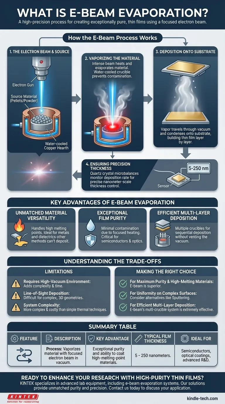
How the E-Beam Process Works
The e-beam evaporation process is a highly controlled sequence that takes place within a high-vacuum environment to ensure the purity of the final film.
The Electron Beam and Source
A beam of electrons is generated and accelerated toward a target material. This material, often in the form of pellets or powder, rests in a water-cooled copper hearth or crucible.
Vaporizing the Material
The intense energy from the electron beam is concentrated on the source material, causing it to rapidly heat, melt, and then evaporate into a vapor. A key advantage is that the water-cooled crucible itself remains cool, preventing contamination of the vapor and ensuring a high-purity film.
Deposition onto the Substrate
The vaporized particles travel upward in straight lines through the vacuum chamber. They eventually reach and condense on the cooler substrate, which is strategically positioned above the source, building the thin film layer by layer.
Ensuring Precision Thickness
To maintain precise control, systems often use quartz crystal microbalances. These devices monitor the rate of deposition in real time, allowing for the creation of films with thicknesses controlled down to the nanometer scale, typically between 5 and 250 nanometers.
Key Advantages of E-Beam Evaporation
E-beam evaporation is chosen over other Physical Vapor Deposition (PVD) methods for several distinct reasons, primarily related to temperature and purity.
Unmatched Material Versatility
The process can generate extremely high temperatures focused on the source material. This makes it ideal for depositing materials with very high melting points, including a wide range of metals and dielectric materials that other methods cannot handle.
Exceptional Film Purity
Because the electron beam heats only the source material and not the crucible holding it, there is minimal contamination. This results in a deposited film of exceptionally high purity, which is critical for sensitive applications like semiconductors and optical coatings.
Efficient Multi-Layer Deposition
Modern e-beam systems can hold multiple crucibles, each with a different source material. This allows for the deposition of several different thin films onto a single substrate in sequence without having to vent the vacuum chamber, drastically improving efficiency.
Understanding the Trade-offs
While powerful, the e-beam process has characteristics that make it unsuitable for certain applications. Understanding these limitations is key to making an informed decision.
Requires a High-Vacuum Environment
The entire process must occur in a high vacuum to prevent the electron beam from scattering and to ensure the vaporized material doesn't react with air. Achieving and maintaining this vacuum adds to the equipment complexity and overall process time.
Line-of-Sight Deposition
The material vapor travels in a straight line from the source to the substrate. This "line-of-sight" characteristic means it can be difficult to uniformly coat substrates with complex, three-dimensional geometries, as some surfaces may be shadowed from the source.
System Complexity
E-beam systems, with their high-voltage electron guns and sophisticated control mechanisms, are generally more complex and costly than simpler thermal evaporation techniques. This makes them better suited for applications where their unique advantages are a necessity.
Making the Right Choice for Your Application
Selecting the correct deposition method depends entirely on the specific requirements of your final product.
- If your primary focus is maximum purity and depositing high-melting-point materials: E-beam evaporation is the superior technical choice due to its focused heating and versatility.
- If your primary focus is achieving a uniform coating on complex, non-flat surfaces: You may need to consider alternative methods like sputtering, which offers more conformal coverage.
- If your primary focus is depositing multiple layers of different materials efficiently: The multi-crucible capability of e-beam systems makes it an extremely effective solution.
Ultimately, e-beam evaporation provides unparalleled control and purity for demanding applications where material performance is non-negotiable.
Summary Table:
| Feature | Description |
|---|---|
| Process | Vaporizes material with a focused electron beam in a vacuum. |
| Key Advantage | Exceptional purity and ability to coat high-melting-point materials. |
| Typical Film Thickness | 5 - 250 nanometers |
| Ideal For | Semiconductors, optical coatings, advanced R&D. |
Ready to enhance your research with high-purity thin films?
KINTEK specializes in advanced lab equipment, including e-beam evaporation systems, to meet the demanding needs of laboratories in material science, electronics, and optics. Our solutions provide the unmatched purity and precision your projects require.
Contact us today to discuss how our e-beam evaporation technology can benefit your specific application.
Visual Guide
Related Products
- Electron Beam Evaporation Coating Oxygen-Free Copper Crucible and Evaporation Boat
- Electron Beam Evaporation Coating Tungsten Crucible and Molybdenum Crucible for High Temperature Applications
- Electron Beam Evaporation Coating Gold Plating Tungsten Molybdenum Crucible for Evaporation
- Electron Beam Evaporation Coating Conductive Boron Nitride Crucible BN Crucible
- E Beam Crucibles Electron Gun Beam Crucible for Evaporation
People Also Ask
- What is the voltage of e-beam evaporation? Achieve Precise Thin-Film Deposition
- What are the applications of electron beams? From Nanoscale Imaging to Industrial Manufacturing
- What is the deposition rate of e-beam evaporation? Control Thin Film Quality and Speed
- What is the container that holds the metal source material called in e-beam evaporation? Ensure Purity and Quality in Your Thin-Film Deposition
- What is the temperature of e-beam evaporation? Mastering the Two-Zone Thermal Process for Precision Films


