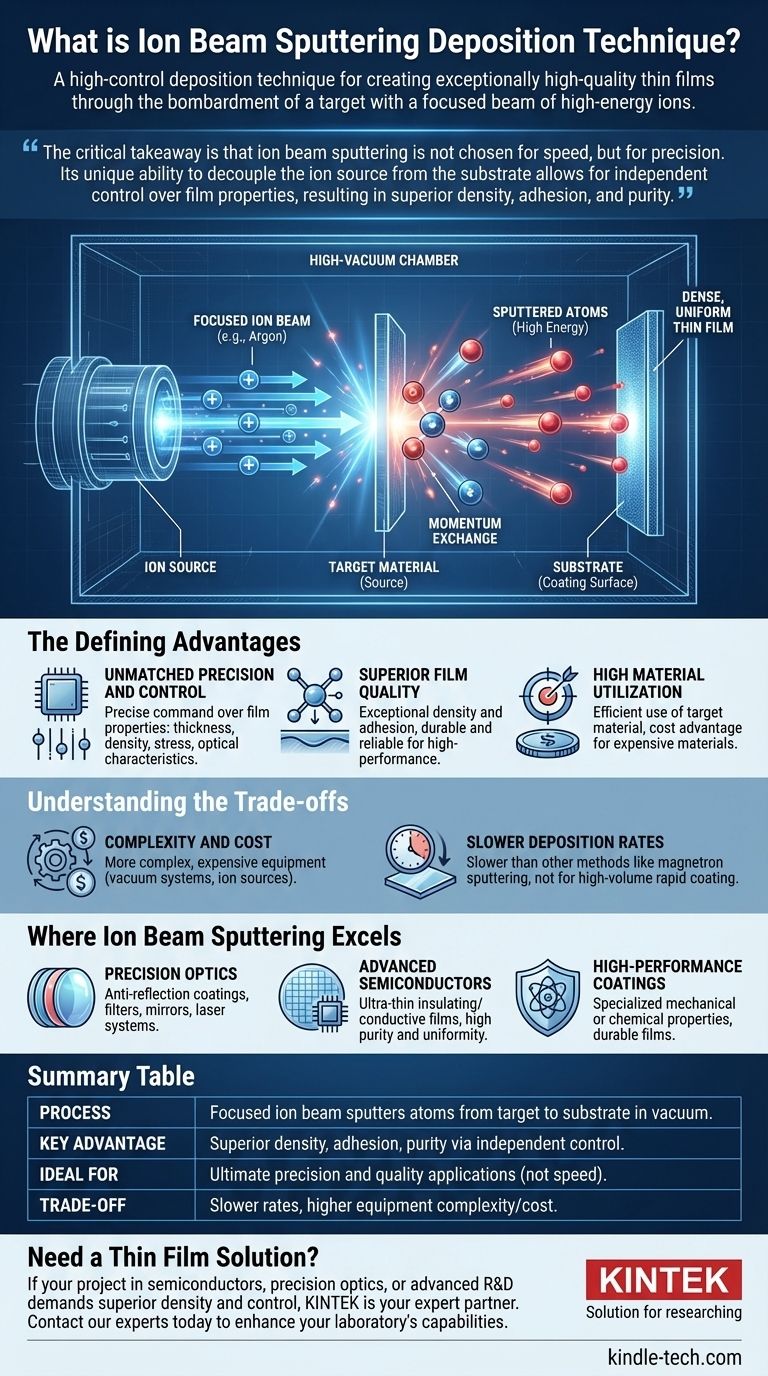
At its core, ion beam sputtering is a highly controlled deposition technique used to create exceptionally high-quality thin films. The process uses a focused beam of high-energy ions, typically from an inert gas like argon, to bombard a target material. This collision dislodges, or "sputters," atoms from the target, which then travel and deposit onto a substrate, forming a dense and uniform film.
The critical takeaway is that ion beam sputtering is not chosen for speed, but for precision. Its unique ability to decouple the ion source from the substrate allows for independent control over film properties, resulting in superior density, adhesion, and purity that other methods struggle to achieve.
How Ion Beam Sputtering Works
The effectiveness of ion beam sputtering lies in its methodical and energetic process, which takes place inside a high-vacuum chamber.
The Ion Source and Vacuum Chamber
The entire process begins by creating a high-vacuum environment to eliminate contaminants. An inert gas, most commonly argon, is introduced into a separate ion source.
This source then uses an electric field to strip electrons from the argon atoms, creating a stream of positively charged ions.
Bombarding the Target
This stream of ions is accelerated and focused into a high-energy beam directed at the source material, known as the target.
When the ions strike the target, they transfer their kinetic energy through a process of momentum exchange. This is analogous to a cue ball striking a rack of billiard balls, but on an atomic scale.
Deposition onto the Substrate
This energy transfer is forceful enough to knock atoms loose from the target material. These ejected atoms have significantly higher energy—often around 10 eV, which is nearly 100 times that of particles in standard evaporation techniques.
These high-energy particles travel through the vacuum and strike the substrate (the material being coated). Their high energy allows them to migrate slightly on the surface, finding optimal positions to form a highly dense, well-adhered, and defect-free film.
The Defining Advantages of This Technique
The separation of the ion source, target, and substrate is what gives this method its distinct advantages over more conventional sputtering techniques.
Unmatched Precision and Control
Because the ion beam's energy, angle, and current can be controlled independently from the substrate, engineers have precise command over the film's properties. This includes thickness, density, stress, and even its optical characteristics.
Superior Film Quality
The high energy of the sputtered particles results in films with exceptional density and strong adhesion to the substrate. This makes them more durable and reliable for high-performance applications.
High Material Utilization
The focused nature of the ion beam allows for very efficient use of the target material, which is a significant cost advantage when working with expensive or exotic materials.
Understanding the Trade-offs
While powerful, ion beam sputtering is not a universal solution. Its primary trade-offs are complexity and speed.
The Cost of Precision
The equipment required for ion beam sputtering is more complex and expensive than for simpler deposition methods. This includes the high-vacuum systems and the sophisticated ion source.
Slower Deposition Rates
The methodical, highly controlled nature of the process generally results in slower deposition rates compared to techniques like magnetron sputtering. This makes it less suitable for applications where high-volume, rapid coating is the primary goal.
Where Ion Beam Sputtering Excels
This technique is reserved for applications where film performance and precision are non-negotiable.
Precision Optics
Ion beam sputtering is critical for creating multi-layer anti-reflection coatings, filters, and mirrors for lenses and laser systems. The precise control over each layer's thickness and refractive index is essential.
Advanced Semiconductors
In semiconductor manufacturing, it is used to deposit ultra-thin insulating or conductive films where purity and uniformity are paramount for device performance.
High-Performance Coatings
The technique is also used to create specialized films with specific mechanical or chemical properties, such as durable nitride films or coatings for sensitive devices like gyroscopes.
Making the Right Choice for Your Goal
Selecting the right deposition technique requires aligning the method's strengths with your project's primary objective.
- If your primary focus is ultimate film quality and density: Ion beam sputtering is the superior choice due to the high particle energy that eliminates voids and ensures strong adhesion.
- If your primary focus is precise control over complex layers: This technique's independent control over deposition parameters makes it ideal for advanced optical or electronic components.
- If your primary focus is high-volume throughput and lower cost: A less complex method like magnetron sputtering is likely a more practical and economical solution.
Ultimately, choosing ion beam sputtering is an investment in achieving a level of quality and precision that other methods simply cannot replicate.
Summary Table:
| Feature | Description |
|---|---|
| Process | A focused ion beam sputters atoms from a target to deposit a thin film on a substrate in a vacuum. |
| Key Advantage | Superior film density, adhesion, and purity due to independent control of ion source and substrate. |
| Ideal For | Applications requiring ultimate precision and quality, not high speed. |
| Trade-off | Slower deposition rates and higher equipment complexity/cost. |
Need a Thin Film Solution with Unmatched Precision?
If your project in semiconductors, precision optics, or advanced R&D demands the superior density and control of ion beam sputtering, KINTEK is your expert partner. We specialize in providing the high-performance lab equipment and consumables you need to achieve flawless results.
Contact our experts today to discuss how our solutions can enhance your laboratory's capabilities.
Visual Guide
Related Products
- Chemical Vapor Deposition CVD Equipment System Chamber Slide PECVD Tube Furnace with Liquid Gasifier PECVD Machine
- Customer Made Versatile CVD Tube Furnace Chemical Vapor Deposition Chamber System Equipment
- RF PECVD System Radio Frequency Plasma-Enhanced Chemical Vapor Deposition RF PECVD
- HFCVD Machine System Equipment for Drawing Die Nano-Diamond Coating
- Custom CVD Diamond Coating for Lab Applications
People Also Ask
- What types of substrates are used in CVD to facilitate graphene films? Optimize Graphene Growth with the Right Catalyst
- How are carbon nanotubes grown? Master Scalable Production with Chemical Vapor Deposition
- Why is Chemical Vapor Deposition (CVD) equipment uniquely suited for constructing hierarchical superhydrophobic structures?
- What is the chemical vapor deposition growth process? Build Superior Thin Films from the Atom Up
- How expensive is chemical vapor deposition? Understanding the True Cost of High-Performance Coating


