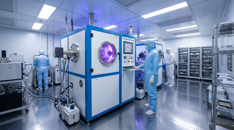
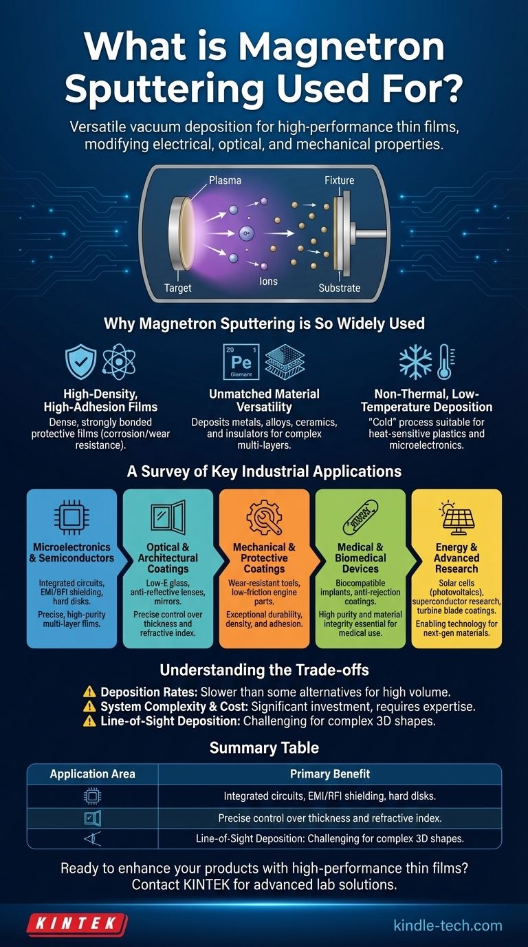
At its core, magnetron sputtering is a highly versatile vacuum deposition technique used to apply extremely thin films of material onto a surface. Industries rely on it to create high-performance coatings that modify an object's electrical, optical, or mechanical properties, from the microchips in your phone and the glass on skyscrapers to advanced medical implants.
Magnetron sputtering's value lies not just in applying a coating, but in its ability to create exceptionally dense, durable, and pure films from a vast range of materials. This precision and control make it a foundational technology for manufacturing advanced products across nearly every major industry.
Why Magnetron Sputtering is So Widely Used
To understand its applications, you must first understand its core capabilities. The process doesn't just "paint" a surface; it physically bombards a target material with energized ions, ejecting atoms that then embed themselves onto the substrate. This mechanism gives the resulting films unique and valuable characteristics.
Creating High-Density, High-Adhesion Films
The energy of the sputtered atoms ensures they form a film that is incredibly dense and strongly bonded to the substrate. This is a fundamental reason for its use in protective applications.
These films provide superior protection against environmental factors, making them ideal for corrosion-resistant coatings on automotive or aerospace components made from materials like magnesium alloys.
The same principle delivers exceptional durability for wear-resistant and low-friction coatings on cutting tools and industrial machinery, significantly extending their operational life.
Unmatched Material Versatility
Magnetron sputtering is not limited to simple metals. The process can deposit a vast library of materials, including pure metals, complex alloys, and even insulating or ceramic compounds.
This versatility is crucial for creating complex devices with multiple layers, each serving a different function. A single product might have layers for electrical conduction, insulation, and optical filtering, all deposited using sputtering.
Non-Thermal, Low-Temperature Deposition
A key advantage of magnetron sputtering is that it is a "cold" process. The substrate remains at or near room temperature, preventing thermal damage.
This makes it the perfect method for coating heat-sensitive materials like plastics, polymers, and complex microelectronics. This is critical for producing displays, flexible electronics, and integrated circuits without damaging the underlying components.
A Survey of Key Industrial Applications
The unique benefits of sputtering have made it an indispensable process across numerous high-tech fields.
Microelectronics and Semiconductors
Sputtering was one of the earliest and still most common methods for manufacturing computer hard disks and processing integrated circuits.
It is used to deposit the ultra-thin, multi-layer metallic films required for on-chip wiring, transistors, and other critical components. It is also used to create EMI/RFI shielding that protects sensitive electronics from interference.
Optical and Architectural Coatings
The process allows for precise control over a film's thickness and refractive index, which is essential for optical applications.
This includes producing low-emissivity (Low-E) glass for energy-efficient buildings, anti-reflective coatings for lenses and displays, and highly reflective films for mirrors and decorative finishes.
Mechanical and Protective Coatings
The durability of sputtered films makes them ideal for surface engineering. Industries rely on sputtering for super-hard films that protect tools and engine parts from wear and tear.
These coatings can also be engineered to be self-lubricating, reducing friction in high-performance mechanical systems.
Medical and Biomedical Devices
In the medical field, purity and material integrity are paramount. Sputtering is used to apply biocompatible coatings to dental implants and other surgical tools.
It can create anti-rejection coatings on devices to prevent allergic reactions and is even used to manufacture components for angioplasty devices and precisely targeted radiation capsules.
Energy and Advanced Research
Sputtering is a key enabling technology for renewable energy, used to deposit the critical layers in solar cells (photovoltaics) and create protective coatings for gas turbine blades.
In research, it is the primary method for exploring and developing next-generation materials, including high-temperature superconductors, ferroelectric films, and thin-film memory alloys.
Understanding the Trade-offs
While powerful, magnetron sputtering is not a universal solution. Understanding its limitations is key to making an informed decision.
Deposition Rates
For some materials, sputtering can be a slower deposition process compared to alternatives like thermal evaporation. This can impact high-volume manufacturing where throughput is the primary driver.
System Complexity and Cost
The vacuum chambers, high-power supplies (especially the RF systems needed for insulators), and magnetic assemblies represent a significant capital investment. The process requires a higher level of technical expertise to operate and maintain compared to simpler coating methods.
Line-of-Sight Deposition
Sputtering is a line-of-sight process, meaning atoms travel in a straight line from the target to the substrate. Coating complex, three-dimensional shapes uniformly can be challenging and often requires sophisticated, multi-axis rotation of the part being coated.
Making the Right Choice for Your Goal
Ultimately, the decision to use magnetron sputtering is driven by the performance requirements of the final product.
- If your primary focus is maximum durability and adhesion: Sputtering is the superior choice for creating dense, wear-resistant, and corrosion-proof protective films.
- If your primary focus is advanced electronics or optics: The precision, purity, and material versatility of sputtering make it the industry standard for complex, multi-layer functional coatings.
- If your primary focus is coating heat-sensitive substrates: Sputtering's non-thermal nature is a critical advantage for plastics, polymers, and delicate electronic assemblies.
- If your primary focus is high-speed, simple coatings: You must weigh the superior quality of sputtered films against the potentially faster deposition rates of other methods like thermal evaporation.
Magnetron sputtering is the enabling technology behind many of the high-performance products that define our modern world.
Summary Table:
| Application Area | Key Use Cases | Primary Benefit |
|---|---|---|
| Microelectronics & Semiconductors | Integrated circuits, EMI/RFI shielding, hard disks | High-purity, precise multi-layer deposition |
| Optical & Architectural Coatings | Low-E glass, anti-reflective films, mirrors | Precise control over thickness and refractive index |
| Mechanical & Protective Coatings | Wear-resistant tools, corrosion-resistant components | Exceptional density, adhesion, and durability |
| Medical & Biomedical Devices | Biocompatible implants, anti-rejection coatings | High purity and material integrity |
| Energy & Advanced Research | Solar cells, superconductors, turbine blade coatings | Versatility for complex material deposition |
Ready to enhance your products with high-performance thin films? KINTEK specializes in advanced lab equipment and consumables for magnetron sputtering, serving industries from microelectronics to medical devices. Our solutions help you achieve superior coating quality, durability, and precision. Contact our experts today to discuss how we can support your laboratory's specific needs!
Visual Guide
Related Products
- Spark Plasma Sintering Furnace SPS Furnace
- RF PECVD System Radio Frequency Plasma-Enhanced Chemical Vapor Deposition RF PECVD
People Also Ask
- What are the advantages of CAMI/SPS for W-Cu composite preparation? Reduce cycles from hours to seconds.
- What are the fundamentals of spark plasma sintering process? Unlock Rapid, High-Performance Material Consolidation
- What is SPS sintering method? A Guide to High-Speed, High-Performance Material Fabrication
- What technical advantages does a Spark Plasma Sintering (SPS) furnace offer for LZP ceramics? Enhance Ionic Conductivity
- What is the difference between spark plasma sintering and flash sintering? A Guide to Advanced Sintering Methods

