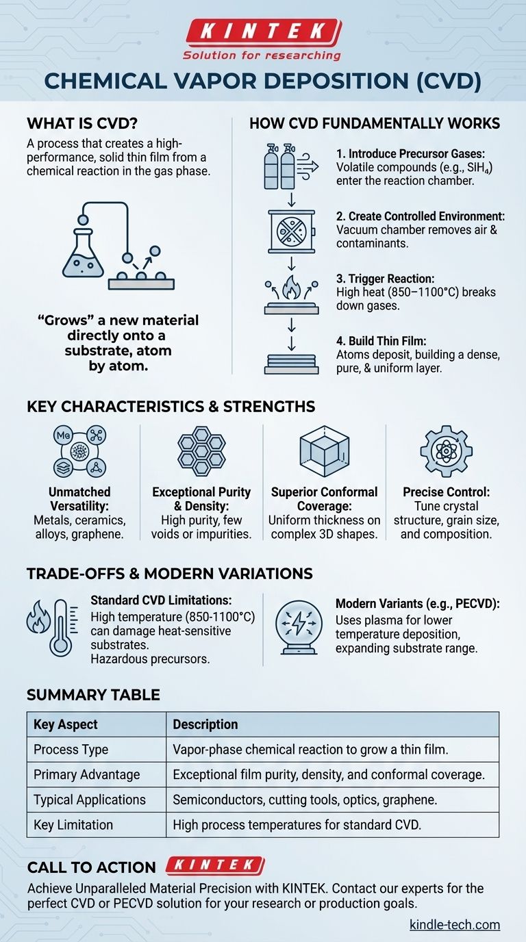
In short, Chemical Vapor Deposition (CVD) is a manufacturing process that creates a high-performance, solid thin film on a surface from a chemical reaction in the gas phase. Inside a vacuum chamber, one or more volatile precursor gases are introduced, which then react or decompose on a heated substrate to form the desired material layer by layer. This method is distinct from simply coating a surface; it grows a new material directly onto the substrate.
The central idea behind CVD is not just to deposit a material, but to synthesize it directly on a surface. By controlling the chemical reaction of gases at a molecular level, CVD builds exceptionally pure, dense, and uniform thin films that are impossible to create with many other methods.
How CVD Fundamentally Works
To truly understand CVD, it's best to think of it as a precise, atom-by-atom construction process occurring within a controlled environment. The process can be broken down into a few key stages.
Step 1: Introducing the Precursor Gases
The process begins with precursor gases, which are volatile compounds containing the atoms needed for the final film. For example, to create a silicon film, a gas like silane (SiH₄) might be used. These gases are precisely metered and introduced into a reaction chamber.
Step 2: Creating a Controlled Environment
The substrate (the workpiece to be coated) is placed inside a vacuum chamber. The vacuum is not used to "pull" the gases, but rather to remove air and other contaminants that could interfere with the chemical reaction and compromise the purity of the final film.
Step 3: Triggering the Chemical Reaction
The substrate is heated to a specific, often very high, reaction temperature (typically 850–1100°C). This thermal energy breaks down the precursor gases on or near the hot substrate surface, releasing the desired atoms. These atoms then bond to the surface.
Step 4: Building the Thin Film
As the reaction continues, atoms continuously deposit onto the substrate, building up a thin film one atomic layer at a time. This results in an exceptionally dense, pure, and uniform coating that grows over the entire exposed surface of the component.
Key Characteristics and Strengths
Engineers and scientists choose CVD when the properties of the final film are paramount. Its unique approach provides several distinct advantages.
Unmatched Material Versatility
CVD is not limited to one type of material. The process can be adapted to deposit a vast range of materials, including metals, ceramics (like silicon nitride), multi-component alloys, and advanced materials like graphene.
Exceptional Purity and Density
Because the film is built from a high-purity gas source in a clean vacuum environment, the resulting layer has extremely high purity and density. It is largely free of the voids or impurities that can plague other coating methods.
Superior Conformal Coverage
Since the precursor is a gas, it flows around and into complex geometries. This gives CVD excellent conformal coverage, meaning it can deposit a film of uniform thickness on intricate, three-dimensional shapes—a significant advantage over line-of-sight processes like Physical Vapor Deposition (PVD).
Precise Control Over Film Properties
By carefully adjusting process parameters like temperature, pressure, and gas flow rates, operators can precisely control the film's final properties. This includes its crystal structure, grain size, and chemical composition, making it a leading method for high-performance electronics where material characteristics are critical.
Understanding the Trade-offs and Limitations
No process is perfect, and the strengths of CVD come with important trade-offs that must be considered for any application.
The High Temperature Requirement
The most significant limitation of standard CVD is the high reaction temperature. Many potential substrate materials, such as plastics or certain metals, cannot withstand the heat and would be damaged or destroyed during the process.
Modern Variations Mitigate Heat
To address this limitation, modern variants have been developed. Plasma-Enhanced CVD (PECVD), for example, uses an electric field to create a plasma, which provides the energy to break down the precursor gases at much lower temperatures, expanding the range of usable substrates.
Hazardous Precursor Materials
The gases used in CVD can be toxic, flammable, or corrosive. This necessitates sophisticated handling systems and stringent safety protocols, which can add to the complexity and cost of the operation.
Making the Right Choice for Your Application
Selecting the right deposition technology depends entirely on your project's specific requirements for film quality, substrate material, and component geometry.
- If your primary focus is ultimate film quality and purity: CVD is often the superior choice for demanding applications in semiconductors, optics, and advanced electronics.
- If your primary focus is coating complex 3D shapes uniformly: The gas-phase nature of CVD provides conformal coverage that line-of-sight processes cannot match.
- If you are working with heat-sensitive substrates: Standard CVD is likely unsuitable, and you must investigate lower-temperature variants like PECVD or alternative processes entirely.
By understanding its core principles and trade-offs, you can leverage CVD to engineer materials with unparalleled precision at the atomic level.
Summary Table:
| Key Aspect | Description |
|---|---|
| Process Type | Vapor-phase chemical reaction to grow a thin film. |
| Primary Advantage | Exceptional film purity, density, and conformal coverage on complex shapes. |
| Typical Applications | Semiconductors, cutting tools, optics, and graphene production. |
| Key Limitation | High process temperatures can damage heat-sensitive substrates. |
Need a high-performance thin film for your application?
The principles of CVD are fundamental to creating the advanced materials that power modern technology. If your project demands exceptional film purity, uniform coverage on complex 3D parts, or precise control over material properties, the right equipment is critical.
KINTEK specializes in lab equipment and consumables, serving laboratory needs. Our expertise can help you select the ideal deposition system, whether it's a standard CVD furnace for high-temperature applications or a Plasma-Enhanced CVD (PECVD) system for heat-sensitive materials.
Let's discuss how we can help you achieve unparalleled material precision. Contact our experts today to find the perfect solution for your research or production goals.
Visual Guide
Related Products
- Chemical Vapor Deposition CVD Equipment System Chamber Slide PECVD Tube Furnace with Liquid Gasifier PECVD Machine
- Microwave Plasma Chemical Vapor Deposition MPCVD Machine System Reactor for Lab and Diamond Growth
- 915MHz MPCVD Diamond Machine Microwave Plasma Chemical Vapor Deposition System Reactor
- Customer Made Versatile CVD Tube Furnace Chemical Vapor Deposition Chamber System Equipment
- HFCVD Machine System Equipment for Drawing Die Nano-Diamond Coating
People Also Ask
- What are the core advantages of PE-CVD in OLED encapsulation? Protect Sensitive Layers with Low-Temp Film Deposition
- How are carbon nanotubes grown? Master Scalable Production with Chemical Vapor Deposition
- How expensive is chemical vapor deposition? Understanding the True Cost of High-Performance Coating
- What is plasma enhanced chemical vapor deposition PECVD equipment? A Guide to Low-Temperature Thin Film Deposition
- What types of substrates are used in CVD to facilitate graphene films? Optimize Graphene Growth with the Right Catalyst


