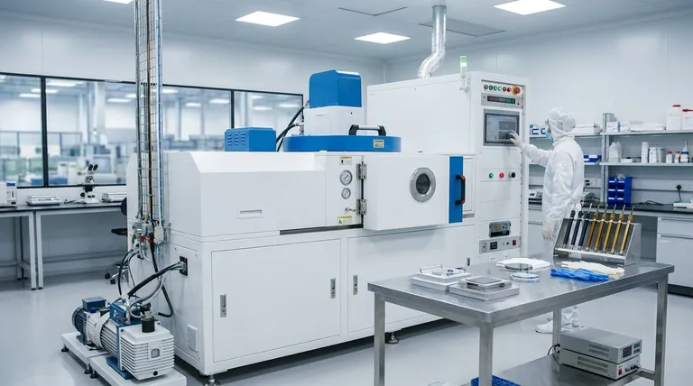
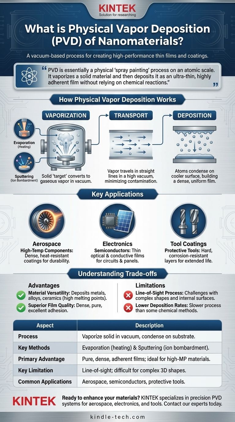
Physical Vapor Deposition (PVD) is a vacuum-based process used to create high-performance thin films and coatings. It works by transforming a solid material into a vapor, which then travels and condenses atom-by-atom onto a target surface, known as a substrate. This method is fundamental to producing nanomaterials and enhancing the properties of everything from semiconductor chips to aerospace components.
PVD is essentially a physical "spray painting" process on an atomic scale. It vaporizes a solid material and then deposits it as an ultra-thin, highly adherent film without relying on chemical reactions to form the final material on the substrate.
How Physical Vapor Deposition Works
The PVD process operates under a high vacuum and can be broken down into three main stages: vaporization of the source material, transport of the vapor, and deposition onto the substrate.
The Vacuum Environment
A vacuum chamber is essential for PVD. It removes air and other gases that could react with the vaporized material or impede its path to the substrate, ensuring a pure and uncontaminated final film.
The Vaporization Step
This is where the solid "target" material is converted into a gaseous vapor. There are two primary methods for achieving this.
- Evaporation: The source material is heated in the vacuum until it evaporates, turning directly into a gas. This is often done using techniques like electron-beam evaporation, common in aerospace applications.
- Sputtering: The source material is bombarded with high-energy ions (typically from an inert gas like argon). This energetic collision physically knocks atoms off the surface of the target, ejecting them into the vacuum chamber.
Deposition on the Substrate
The vaporized atoms travel in a straight line from the source to the substrate. Upon arrival, they condense on the cooler surface, gradually building a thin, dense, and uniform film.
Key Applications of PVD
The unique capabilities of PVD make it a critical technology across many advanced industries for applying specialized coatings.
Aerospace and High-Temperature Components
PVD is used to apply dense, temperature-resistant coatings to parts like turbine blades. These films enhance durability and protect components from the extreme heat and stress of operation.
Electronics and Semiconductors
In the electronics industry, PVD applies the thin optical and conductive films necessary for solar panels and integrated circuits. This precise control at the atomic level is vital for modern microelectronics.
Protective Tool Coatings
Hard, corrosion-resistant coatings are applied to cutting tools, drills, and molds using PVD. This significantly extends the life and performance of tools used in harsh industrial environments.
Understanding the Trade-offs
While powerful, PVD is not the solution for every application. Understanding its advantages and limitations is key to using it effectively.
Advantage: Material Versatility
PVD can deposit a vast range of materials, including metals, alloys, and ceramics. It is particularly effective for materials with very high melting points that are difficult to process with other methods.
Advantage: Superior Film Quality
The resulting films are typically very dense, pure, and have excellent adhesion to the substrate. This creates a durable and reliable coating.
Limitation: Line-of-Sight Process
Because the vapor travels in a straight line, PVD can only coat surfaces that have a direct, unobstructed path from the source. This makes it challenging to uniformly coat complex shapes with internal surfaces or undercuts.
Limitation: Lower Deposition Rates
Compared to some chemical methods, PVD can be a slower process. This can be a consideration for high-volume manufacturing where throughput is a primary concern.
Making the Right Choice for Your Goal
The decision to use PVD depends entirely on the material properties and surface geometry your project requires.
- If your primary focus is creating a pure, dense coating on a relatively simple surface: PVD is an excellent choice, especially for materials with high melting points.
- If your primary focus is applying a highly durable, wear-resistant layer to tools: PVD techniques are the industry standard for creating hard, protective coatings.
- If your primary focus is uniformly coating a complex, three-dimensional object: You should investigate Chemical Vapor Deposition (CVD), a process that uses gas-phase chemical reactions and does not have the line-of-sight limitations of PVD.
Understanding the fundamental mechanism of PVD—vaporize, travel, condense—is the key to leveraging its power for advanced material engineering.
Summary Table:
| Aspect | Description |
|---|---|
| Process | Vaporizes a solid material in a vacuum, which then condenses atom-by-atom onto a substrate. |
| Key Methods | Evaporation (heating) and Sputtering (bombarding with ions). |
| Primary Advantage | Creates pure, dense, and highly adherent films; ideal for high-melting-point materials. |
| Key Limitation | Line-of-sight process, making it challenging to coat complex 3D shapes uniformly. |
| Common Applications | Aerospace components, semiconductor chips, and protective tool coatings. |
Ready to enhance your materials with high-performance thin films?
KINTEK specializes in precision lab equipment, including PVD systems, to help you develop superior coatings for aerospace, electronics, and industrial tools. Our expertise ensures you get the right solution for creating pure, durable, and high-adhesion films.
Contact our experts today to discuss how our PVD technology can meet your specific laboratory and R&D needs.
Visual Guide
Related Products
- Chemical Vapor Deposition CVD Equipment System Chamber Slide PECVD Tube Furnace with Liquid Gasifier PECVD Machine
- RF PECVD System Radio Frequency Plasma-Enhanced Chemical Vapor Deposition RF PECVD
- Customer Made Versatile CVD Tube Furnace Chemical Vapor Deposition Chamber System Equipment
- Microwave Plasma Chemical Vapor Deposition MPCVD Machine System Reactor for Lab and Diamond Growth
- Custom CVD Diamond Coating for Lab Applications
People Also Ask
- How expensive is chemical vapor deposition? Understanding the True Cost of High-Performance Coating
- Why is Chemical Vapor Deposition (CVD) equipment uniquely suited for constructing hierarchical superhydrophobic structures?
- What is the chemical vapor deposition growth process? Build Superior Thin Films from the Atom Up
- What types of substrates are used in CVD to facilitate graphene films? Optimize Graphene Growth with the Right Catalyst
- What happens during deposition chemistry? Building Thin Films from Gaseous Precursors


