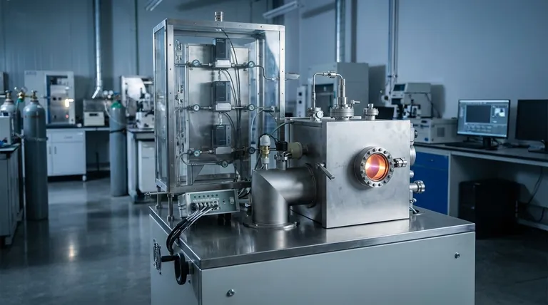
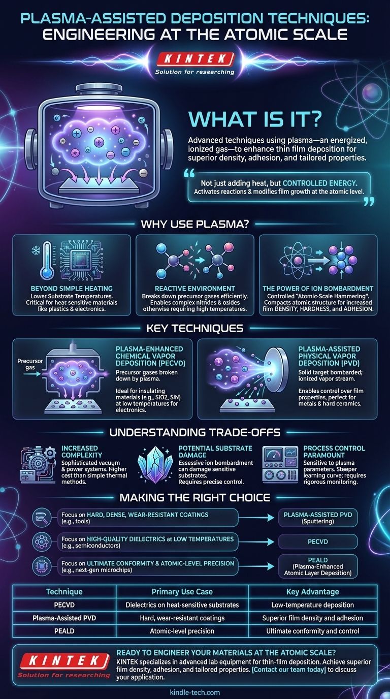
In essence, plasma-assisted deposition is a family of advanced techniques used to create high-performance thin films and coatings. These methods use plasma—an energized, ionized gas—to fundamentally enhance the deposition process, allowing for the creation of materials with superior density, adhesion, and tailored properties that are often impossible to achieve with conventional thermal or chemical methods alone.
The central purpose of using plasma in deposition is not just to add heat, but to add controlled energy. This energy activates chemical reactions and physically modifies the film as it grows, providing precise control over the final material's structure and performance.
Why Use Plasma in Deposition?
Traditional deposition methods often rely on high temperatures to provide the energy needed for chemical reactions or material evaporation. Plasma offers a more sophisticated way to energize the system, unlocking significant advantages.
Beyond Simple Heating
Instead of just making things hot, plasma creates a unique environment filled with a high-energy soup of ions, electrons, and reactive neutral particles. This allows processes to occur at much lower substrate temperatures, which is critical when coating heat-sensitive materials like plastics or complex electronics.
Creating a Reactive Environment
The plasma efficiently breaks down precursor gases into their most reactive components. This allows for the formation of complex materials, such as nitrides or oxides, that would otherwise require extremely high temperatures or less stable chemical precursors.
The Power of Ion Bombardment
Positively charged ions within the plasma can be accelerated toward the substrate surface. This controlled "atomic-scale hammering" or ion bombardment has a profound effect on the growing film. It compacts the atomic structure, dramatically increasing the film's density, hardness, and adhesion to the underlying surface.
Key Plasma-Assisted Techniques
Plasma is not a single tool but a versatile energy source applied to different deposition frameworks. The two most prominent categories are based on whether the source material starts as a gas or a solid.
Plasma-Enhanced Chemical Vapor Deposition (PECVD)
In PECVD, precursor gases are introduced into a chamber where a plasma breaks them down. These reactive fragments then settle on the substrate to form the desired film. This technique is ideal for depositing insulating materials like silicon dioxide or silicon nitride at low temperatures for the electronics industry.
Plasma-Assisted Physical Vapor Deposition (PVD)
In PVD, the source material starts as a solid target. Plasma is used to bombard this target, knocking atoms off of it in a process called sputtering. The plasma can also be used to ionize this vapor stream as it travels to the substrate, enabling greater control over the film's properties upon arrival. This is where benefits like improved film properties and control over a wider range of materials, especially metals and hard ceramics, truly shine.
Understanding the Trade-offs
While powerful, plasma-assisted techniques introduce complexities that must be managed to achieve their full potential.
Increased System Complexity
Generating and sustaining a stable plasma requires sophisticated equipment, including vacuum chambers, power supplies, and gas handling systems. This inherently increases the cost and complexity compared to simpler methods like thermal evaporation.
Potential for Substrate Damage
The same ion bombardment that improves film density can, if not precisely controlled, cause damage to the crystal structure of sensitive substrates. Balancing the beneficial effects with potential damage is a key challenge of process development.
Process Control is Paramount
The final film properties are exquisitely sensitive to plasma parameters like power, pressure, and gas composition. Achieving repeatable, high-quality results demands greater control over the deposition process, but this also means there is a steeper learning curve and a need for rigorous process monitoring.
Making the Right Choice for Your Goal
Selecting a deposition method depends entirely on the required film properties and the nature of the substrate.
- If your primary focus is hard, dense, wear-resistant coatings (e.g., for cutting tools): Plasma-assisted PVD techniques like sputtering are the industry standard.
- If your primary focus is depositing high-quality dielectrics at low temperatures (e.g., on semiconductors or plastics): PECVD is the superior choice.
- If your primary focus is ultimate conformity and atomic-level precision (e.g., for next-gen microchips): You should investigate Plasma-Enhanced Atomic Layer Deposition (PEALD).
By leveraging plasma, you are fundamentally moving from simple coating to actively engineering a material's properties at the atomic scale.
Summary Table:
| Technique | Primary Use Case | Key Advantage |
|---|---|---|
| PECVD | Dielectrics on heat-sensitive substrates | Low-temperature deposition |
| Plasma-Assisted PVD | Hard, wear-resistant coatings | Superior film density and adhesion |
| PEALD | Atomic-level precision | Ultimate conformity and control |
Ready to Engineer Your Materials at the Atomic Scale?
Whether you are developing next-generation semiconductors, durable industrial coatings, or advanced optical films, the right plasma-assisted deposition system is critical to your success. KINTEK specializes in advanced lab equipment for thin-film deposition, providing the precise control and reliability your research and production demand.
Let our experts help you select the perfect solution to achieve superior film density, adhesion, and tailored properties.
Contact our team today to discuss your specific application and discover how KINTEK can empower your innovation.
Visual Guide
Related Products
- Chemical Vapor Deposition CVD Equipment System Chamber Slide PECVD Tube Furnace with Liquid Gasifier PECVD Machine
- 915MHz MPCVD Diamond Machine Microwave Plasma Chemical Vapor Deposition System Reactor
- RF PECVD System Radio Frequency Plasma-Enhanced Chemical Vapor Deposition RF PECVD
- Microwave Plasma Chemical Vapor Deposition MPCVD Machine System Reactor for Lab and Diamond Growth
- Cylindrical Resonator MPCVD Machine System Reactor for Microwave Plasma Chemical Vapor Deposition and Lab Diamond Growth
People Also Ask
- Why is Chemical Vapor Deposition (CVD) equipment uniquely suited for constructing hierarchical superhydrophobic structures?
- What are the core advantages of PE-CVD in OLED encapsulation? Protect Sensitive Layers with Low-Temp Film Deposition
- What is plasma enhanced chemical vapor deposition PECVD equipment? A Guide to Low-Temperature Thin Film Deposition
- What are the advantages of chemical vapor deposition? Achieve Superior Thin Films for Your Lab
- How are carbon nanotubes grown? Master Scalable Production with Chemical Vapor Deposition


