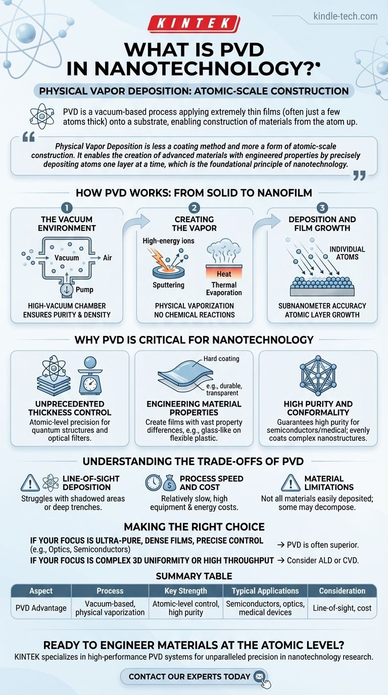
In nanotechnology, PVD stands for Physical Vapor Deposition. It is a vacuum-based process used to apply extremely thin films of material—often just a few atoms thick—onto a surface, or substrate. This technique is fundamental to nanotechnology because it allows engineers and scientists to construct materials from the atom up, giving them precise control over the final product's properties like durability, conductivity, and optical behavior.
Physical Vapor Deposition is less a coating method and more a form of atomic-scale construction. It enables the creation of advanced materials with engineered properties by precisely depositing atoms one layer at a time, which is the foundational principle of nanotechnology.
How PVD Works: From Solid to Nanofilm
PVD encompasses a family of techniques, but they all share the same core principle: turning a solid material into a vapor within a vacuum, transporting it, and condensing it onto a target substrate to form a solid film.
The Vacuum Environment
The entire PVD process happens inside a high-vacuum chamber. This is critical because it removes air and other particles that could contaminate the film or interfere with the vaporized atoms as they travel.
A near-perfect vacuum ensures the resulting nanofilm is exceptionally pure and dense.
Creating the Vapor (The "Physical" Step)
The "physical" in PVD refers to the method used to vaporize the source material, or "target." This is done without chemical reactions.
The two most common methods are sputtering, where the target is bombarded with high-energy ions that knock atoms loose, and thermal evaporation, where the material is heated until it boils and releases atoms as a vapor.
Deposition and Film Growth
Once vaporized, the individual atoms travel in a straight line through the vacuum chamber until they strike the cooler substrate.
Upon impact, they condense and begin to form a thin film. By precisely controlling the process duration and conditions, operators can achieve subnanometer-level accuracy, building the film layer by atomic layer.
Why PVD is Critical for Nanotechnology
PVD isn't just a coating process; it's an enabling technology. Its precision is what allows for the practical manufacturing of nanoscale devices and materials.
Unprecedented Thickness Control
The ability to control film thickness with atomic-level precision is paramount. This allows for the creation of structures like quantum wells in semiconductors or specialized optical filters where performance is dictated by a film being an exact number of atoms thick.
Engineering Material Properties
PVD allows us to create films with properties vastly different from the source material. By controlling the film's nanostructure, we can engineer its macro-level characteristics.
For example, a durable, scratch-resistant, and transparent film can be deposited onto flexible plastic, giving it glass-like properties without the brittleness. This is essential for advanced electronics, medical implants, and optics.
High Purity and Conformality
The vacuum environment guarantees a film of very high purity, which is critical for semiconductor and medical applications.
PVD also offers excellent conformality, meaning it can evenly coat the surfaces of complex, three-dimensional nanostructures, ensuring uniform performance across an entire device.
Understanding the Trade-offs of PVD
While powerful, PVD is not a universal solution. Understanding its limitations is key to using it effectively.
Line-of-Sight Deposition
PVD is primarily a line-of-sight process. The vaporized atoms travel in straight lines, which means they can struggle to coat the "shadowed" areas or deep, narrow trenches of highly complex 3D structures.
Process Speed and Cost
Achieving the necessary high vacuum and precisely controlling the deposition rate can make PVD a relatively slow process compared to chemical methods.
Furthermore, PVD equipment represents a significant capital investment and requires substantial energy to operate, making it more suitable for high-value applications.
Material Limitations
While versatile, not all materials can be easily deposited using PVD. Some compounds may decompose when heated, or they may be difficult to sputter effectively, requiring alternative deposition techniques.
Making the Right Choice for Your Goal
Selecting a deposition method depends entirely on the technical and economic requirements of your specific application.
- If your primary focus is creating ultra-pure, dense films with precise atomic-level thickness control (e.g., for advanced optics, semiconductors, or hard coatings): PVD is often the superior choice due to its physical nature and clean vacuum environment.
- If your primary focus is uniformly coating highly complex 3D nanostructures or achieving higher throughput for less sensitive applications: You may need to evaluate alternatives like Atomic Layer Deposition (ALD) for conformality or Chemical Vapor Deposition (CVD) for speed.
Ultimately, PVD is a foundational tool that gives us the power to build the future, one atom at a time.
Summary Table:
| Aspect | PVD Advantage |
|---|---|
| Process | Vacuum-based, physical vaporization (sputtering/evaporation) |
| Key Strength | Atomic-level thickness control and high-purity films |
| Typical Applications | Semiconductors, advanced optics, hard coatings, medical devices |
| Consideration | Line-of-sight limitation; higher equipment and energy costs |
Ready to engineer materials at the atomic level? KINTEK specializes in high-performance lab equipment, including PVD systems, to help you achieve unparalleled precision in your nanotechnology research and development. Our expertise ensures you get the right tools for creating ultra-pure, durable thin films. Contact our experts today to discuss how we can support your laboratory's specific needs.
Visual Guide
Related Products
- RF PECVD System Radio Frequency Plasma-Enhanced Chemical Vapor Deposition RF PECVD
- Split Chamber CVD Tube Furnace with Vacuum Station Chemical Vapor Deposition System Equipment Machine
- Chemical Vapor Deposition CVD Equipment System Chamber Slide PECVD Tube Furnace with Liquid Gasifier PECVD Machine
- VHP Sterilization Equipment Hydrogen Peroxide H2O2 Space Sterilizer
- 30T 40T Split Automatic Heated Hydraulic Press Machine with Heated Plates for Laboratory Hot Press
People Also Ask
- Why is PECVD environment friendly? Understanding the Eco-Friendly Benefits of Plasma-Enhanced Coating
- How does RF power create plasma? Achieve Stable, High-Density Plasma for Your Applications
- How are PECVD and CVD different? A Guide to Choosing the Right Thin-Film Deposition Process
- Why does PECVD commonly use RF power input? For Precise Low-Temperature Thin Film Deposition
- What is an example of PECVD? RF-PECVD for High-Quality Thin Film Deposition