In semiconductor manufacturing, PVD stands for Physical Vapor Deposition, a highly controlled process used to deposit extremely thin layers of metal or other materials onto a silicon wafer. This technique is not merely a coating; it is the fundamental method for building the microscopic metal wiring, known as interconnects, that connects the billions of transistors on a modern microchip, allowing the device to function.
PVD is the critical link between the individual components etched into silicon and the final, functional integrated circuit. It's the technology used to construct the multi-layered "highway system" of wiring that allows electricity and data to travel across a chip.
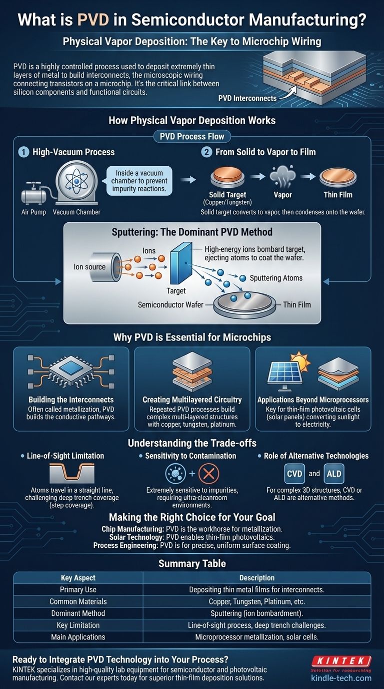
How Physical Vapor Deposition Works
A High-Vacuum Process
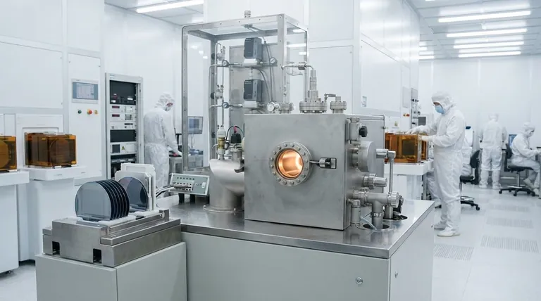
PVD is always performed inside a vacuum chamber. Removing nearly all the air is critical to prevent the deposition material from reacting with oxygen or other particles, which would create impurities and cause defects in the final chip.
From Solid to Vapor to Film
The core principle of PVD involves three steps. First, a solid source material, known as a "target" (e.g., a block of pure copper or tungsten), is converted into a vapor. This vapor then travels through the vacuum and condenses onto the cooler surface of the semiconductor wafer, forming a thin, uniform film.
Sputtering: The Dominant PVD Method
While there are several PVD methods, sputtering is the most common in semiconductor fabrication. In this process, the target is bombarded with high-energy ions (typically from a gas like argon). This bombardment acts like a microscopic sandblaster, ejecting or "sputtering" individual atoms from the target, which then go on to coat the wafer.
Why PVD is Essential for Microchips
Building the Interconnects
After transistors are created within the silicon, the chip is essentially a collection of disconnected switches. PVD is the process, often called metallization, used to build the intricate, multi-layered network of conductive pathways that wire these transistors together into a complex circuit.
Creating Multilayered Circuitry
A modern microprocessor can have over a dozen layers of metal wiring stacked on top of each other, separated by insulating materials. The PVD process is repeated for each layer to build this complex three-dimensional structure. Common metals deposited include copper, tungsten, and platinum.
Applications Beyond Microprocessors
PVD is a versatile technology used across the semiconductor industry. It is a key process in manufacturing thin-film photovoltaic cells (solar panels), where materials like copper, indium, and gallium are deposited onto glass or plastic to create the layers that convert sunlight into electricity.
Understanding the Trade-offs
The "Line-of-Sight" Limitation
Sputtering is a line-of-sight process, meaning the vaporized atoms travel in a relatively straight line from the target to the wafer. This can make it difficult to uniformly coat the bottom and sides of very deep, narrow trenches or holes in the chip's topography, a challenge known as "step coverage."
Sensitivity to Contamination
The process is extremely sensitive to impurities. Any stray particles or molecules inside the vacuum chamber can become embedded in the thin film, potentially causing a short circuit or a complete failure of the chip. This is why PVD occurs in ultra-cleanroom environments.
The Role of Alternative Technologies
For applications where the line-of-sight limitation is a major problem, engineers often turn to other methods like Chemical Vapor Deposition (CVD) or Atomic Layer Deposition (ALD), which can deposit films more conformally over complex 3D structures.
Making the Right Choice for Your Goal
- If your primary focus is chip manufacturing: Understand that PVD is the workhorse technology for metallization, responsible for creating the vast network of metal interconnects.
- If your primary focus is solar technology: Recognize PVD as a key enabler for thin-film photovoltaics, used to build the active layers that capture solar energy.
- If your primary focus is process engineering: View PVD as a precise but line-of-sight-limited technique, best suited for applications where uniform surface coating is the primary goal.
Ultimately, Physical Vapor Deposition is the foundational technique that transforms isolated silicon components into a fully integrated and functional electronic circuit.
Summary Table:
| Key Aspect | Description |
|---|---|
| Primary Use | Depositing thin metal films to create interconnects (wiring) on semiconductor wafers. |
| Common Materials | Copper, Tungsten, Platinum, and other metals. |
| Dominant Method | Sputtering, where a target material is bombarded with ions to eject atoms. |
| Key Limitation | Line-of-sight process, which can challenge coating deep, narrow trenches uniformly. |
| Main Applications | Microprocessor metallization, thin-film solar cells (photovoltaics). |
Ready to Integrate PVD Technology into Your Process?
Whether you are developing next-generation microchips or high-efficiency solar panels, the right lab equipment is critical for precise PVD research and development. KINTEK specializes in providing high-quality lab equipment and consumables tailored to semiconductor and photovoltaic manufacturing needs.
Contact our experts today to discuss how our solutions can help you achieve superior thin-film deposition, enhance your process efficiency, and accelerate your time-to-market.
Visual Guide
Related Products
- Inclined Rotary Plasma Enhanced Chemical Vapor Deposition PECVD Equipment Tube Furnace Machine
- Vacuum Hot Press Furnace Machine for Lamination and Heating
- 915MHz MPCVD Diamond Machine Microwave Plasma Chemical Vapor Deposition System Reactor
- HFCVD Machine System Equipment for Drawing Die Nano-Diamond Coating
- Laboratory Sterilizer Lab Autoclave Pulse Vacuum Lifting Sterilizer
People Also Ask
- What is plasma enhanced chemical vapour deposition process? Unlock Low-Temperature, High-Quality Thin Films
- What is plasma enhanced chemical vapor deposition? Achieve Low-Temperature, High-Quality Thin Films
- What is the difference between PECVD and CVD? Unlock the Right Thin-Film Deposition Method
- What materials are deposited in PECVD? Discover the Versatile Thin-Film Materials for Your Application
- What is PECVD silicon deposition? Achieve Low-Temperature, High-Quality Thin Films