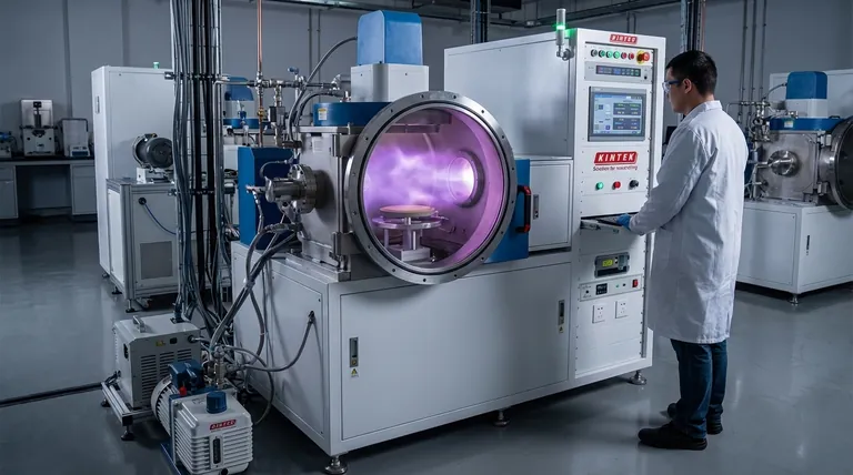
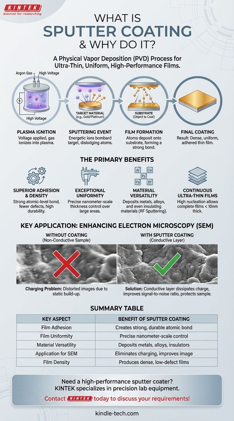
Sputter coating is a physical vapor deposition (PVD) process used to apply an exceptionally thin and uniform layer of material onto a surface. It works by creating a plasma in a vacuum chamber, which bombards a source material (the "target") with energetic ions, dislodging atoms that then deposit onto the object being coated. This technique is used to grant a surface new properties, most notably to make non-conductive materials conductive for analysis or to create highly durable functional films.
At its core, sputter coating is an atomic-level deposition method. It uses momentum to physically knock atoms off a source material, resulting in a film that is far denser, more uniform, and has stronger adhesion than coatings applied through simple evaporation or chemical processes.
How Sputter Coating Works: From Plasma to Film
To understand why sputtering is chosen for high-performance applications, you must first understand its unique physical mechanism. The process is not a chemical reaction or a simple melting and freezing; it is a momentum transfer event.
The Core Components: Target, Substrate, and Gas
The process takes place in a vacuum chamber containing three key elements. The target is a solid piece of the material you want to deposit (like gold or platinum). The substrate is the object you want to coat. Finally, an inert gas, typically argon, is introduced into the chamber.
Igniting the Plasma
A high voltage is applied between the target (acting as a cathode) and an anode. This electrical field energizes the argon gas, stripping electrons from the argon atoms and creating a plasma—an ionized gas containing positive argon ions and free electrons.
The Sputtering Event
The positively charged argon ions are forcefully accelerated toward the negatively charged target. They collide with the target surface with such high energy that they physically knock out, or "sputter," individual atoms from the target material.
Film Formation and Adhesion
These ejected atoms travel through the chamber and land on the substrate. Because they arrive with significant energy, they form an extremely strong, atomic-level bond with the substrate's surface, becoming a permanent part of it. This results in a film that is dense, pure, and highly uniform.
The Primary Benefits of Sputtering
Engineers and scientists choose sputter coating when the quality and performance of the thin film are critical. The physical nature of the process yields several key advantages.
Superior Adhesion and Density
Unlike processes where a material is simply melted and evaporated, sputtered particles impact the substrate with high kinetic energy. This creates a much stronger bond and a denser film with fewer defects, leading to greater durability and better performance.
Exceptional Uniformity and Thickness Control
The sputtering process allows for highly precise control over the film's thickness, often down to the nanometer scale. By managing the input current and deposition time, you can achieve incredibly uniform films over large surface areas.
Material Versatility
While simple DC sputtering works for conductive metals, more advanced techniques like RF (Radio Frequency) sputtering make it possible to deposit films from insulating materials, alloys, and even complex compounds. This versatility opens up a vast range of applications.
Creating Continuous Ultra-Thin Films
The high energy of sputtered atoms leads to a high nucleation density on the substrate. This allows for the formation of complete, continuous films at thicknesses of 10 nanometers or less, a feat that is difficult with other methods.
A Key Application: Enhancing Electron Microscopy
One of the most common uses for sputter coating is in sample preparation for Scanning Electron Microscopy (SEM). Many biological or ceramic samples are not electrically conductive.
Solving the Charging Problem
An electron beam hitting a non-conductive sample in an SEM will cause a build-up of static charge, severely distorting the image. Applying a thin, conductive layer of gold or platinum via sputter coating provides a path for this charge to dissipate, enabling clear imaging.
Improving Image Quality
The sputtered metal coating also dramatically improves the emission of secondary electrons—the primary signal used to form an SEM image. This increases the signal-to-noise ratio, resulting in sharper, more detailed images of the sample's surface topography.
Protecting Sensitive Samples
The electron beam in an SEM can cause thermal damage to delicate specimens. The conductive metal coating helps to spread this thermal load, protecting the underlying sample structure from being altered or destroyed during analysis.
Making the Right Choice for Your Goal
Deciding to use sputter coating depends entirely on the functional requirements of the finished product or the analytical goal.
- If your primary focus is sample analysis (SEM): Sputter coating is an essential preparation step for any non-conductive material, ensuring clear, high-resolution imaging without charge-related artifacts.
- If your primary focus is creating durable, functional films: Sputtering provides a dense and strongly bonded coating ideal for optical filters, microelectronics, and wear-resistant surfaces.
- If your primary focus is precise, uniform coatings: The high degree of control over film thickness and uniformity makes sputtering a superior choice for applications demanding consistency across a surface.
Ultimately, sputter coating is the technique of choice when the physical integrity, performance, and precision of a thin film are paramount.
Summary Table:
| Key Aspect | Benefit of Sputter Coating |
|---|---|
| Film Adhesion | Creates a strong, atomic-level bond for durable coatings |
| Film Uniformity | Enables precise, nanometer-scale thickness control |
| Material Versatility | Can deposit metals, alloys, and insulating materials |
| Application for SEM | Eliminates charging, improves image quality, protects samples |
| Film Density | Produces dense, low-defect films superior to evaporated coatings |
Need a high-performance sputter coater for your lab?
KINTEK specializes in precision lab equipment, including sputter coaters designed to meet the rigorous demands of SEM sample preparation and advanced thin-film research. Our systems deliver the exceptional uniformity, adhesion, and material versatility detailed in this article, ensuring your samples are perfectly prepared for clear, high-resolution imaging and your functional coatings meet the highest standards of durability.
Let our experts help you select the ideal sputtering solution for your specific application. Contact KINTEK today to discuss your requirements and enhance your laboratory's capabilities!
Visual Guide
Related Products
- HFCVD Machine System Equipment for Drawing Die Nano-Diamond Coating
- Electron Beam Evaporation Coating Oxygen-Free Copper Crucible and Evaporation Boat
- 400-700nm Wavelength Anti Reflective AR Coating Glass
People Also Ask
- What is the chemical vapor deposition growth process? Build Superior Thin Films from the Atom Up
- How expensive is chemical vapor deposition? Understanding the True Cost of High-Performance Coating
- What types of substrates are used in CVD to facilitate graphene films? Optimize Graphene Growth with the Right Catalyst
- What are the disadvantages and challenges of the HFCVD method? Overcome Growth Limits and Filament Issues
- What are the advantages of chemical vapor deposition? Achieve Superior Thin Films for Your Lab


