At its core, the sputtering effect is a physical process where atoms are ejected from a solid material—called a target—after it is bombarded by energetic particles. This phenomenon is not random; it is the fundamental mechanism behind sputter deposition, a widely used vacuum technique for applying extremely thin, high-performance coatings onto surfaces like glass, silicon wafers, or plastics.
Sputtering is best understood not just as an "effect," but as a highly controlled manufacturing process. It uses an energized gas plasma to create a vapor from a solid source material, which then condenses onto a substrate to form a uniform and precisely engineered thin film.
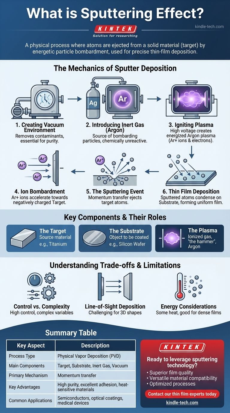
The Mechanics of Sputter Deposition
To truly understand the sputtering effect, you must visualize it as a sequence of events happening inside a vacuum chamber. Each step is critical for producing a high-quality film.
Step 1: Creating the Vacuum Environment
The entire process occurs in a vacuum chamber. This is essential to remove air and other particles that could contaminate the film or interfere with the sputtering process.
Step 2: Introducing an Inert Gas
A small, controlled amount of an inert gas, most commonly Argon (Ar), is introduced into the chamber. This gas will not react chemically with the target material; its sole purpose is to be the source of the bombarding particles.
Step 3: Igniting the Plasma
A strong electric field is applied within the chamber, with the target material acting as the negative cathode and the substrate (the object to be coated) acting as the positive anode. This high voltage strips electrons from the Argon atoms, creating a plasma—a glowing, energized state of matter consisting of positive Argon ions (Ar+) and free electrons.
Step 4: Ion Bombardment
The positively charged Argon ions are forcefully accelerated by the electric field and drawn towards the negatively charged target surface at very high speeds.
Step 5: The Sputtering Event
Upon impact, the energetic Argon ions transfer their momentum to the atoms of the target material. This sets off a "collision cascade" within the target's atomic lattice. When this chain reaction reaches the surface, it ejects target atoms with enough energy to overcome their surface binding forces.
This ejection of atoms from the target is the sputtering effect.
Step 6: Thin Film Deposition
The sputtered atoms travel through the vacuum chamber and land on the substrate. As they accumulate, they condense and build up, atom by atom, to form a thin, solid film with a precisely controlled thickness and structure.
Key Components and Their Roles
The process relies on a few core components working in concert.
The Target
This is the source material for the film. It is a solid block or plate of the material you wish to deposit, such as titanium, aluminum, or silicon dioxide.
The Substrate
This is the object you are coating. The versatility of sputtering allows for a wide range of substrates, from semiconductor wafers and architectural glass to medical implants and plastic components.
The Plasma
The ionized gas (e.g., Argon plasma) acts as the "hammer." It provides the energetic ions needed to bombard the target and initiate the sputtering effect.
Understanding the Trade-offs and Limitations
While powerful, sputtering is a process with specific characteristics that you must consider.
Control vs. Complexity
Sputtering offers unparalleled control over film properties like density, grain structure, and purity. However, this control comes from managing several variables—gas pressure, voltage, and power—making the process more complex than simpler methods like thermal evaporation.
Line-of-Sight Deposition
In its basic form, sputtering is a line-of-sight process. The sputtered atoms travel in relatively straight lines from the target to the substrate. This can make it challenging to achieve a uniform coating on complex, three-dimensional shapes without sophisticated substrate rotation and fixtures.
Energy Considerations
The bombardment of the substrate by various particles in the plasma can impart some heat. While sputtering is considered a "cold" process compared to thermal evaporation, it can still affect extremely heat-sensitive substrates. The energy can also be a benefit, promoting the growth of dense, well-adhered films.
Making the Right Choice for Your Goal
Understanding the sputtering effect helps you decide when and how to leverage it for a specific engineering outcome.
- If your primary focus is creating highly pure and dense films: Sputtering is an excellent choice due to the clean vacuum environment and the energetic deposition process.
- If your primary focus is coating heat-sensitive materials like plastics: Sputtering is often preferred over high-temperature methods because it transfers significantly less heat to the substrate.
- If your primary focus is achieving specific electrical or optical properties: The fine-grained control of sputtering allows for the precise tuning of film characteristics like resistivity, reflectivity, and transparency.
Grasping the sputtering effect transforms your perspective from simply knowing a definition to understanding a powerful tool for advanced material engineering.
Summary Table:
| Key Aspect | Description |
|---|---|
| Process Type | Physical vapor deposition (PVD) using energetic particle bombardment |
| Main Components | Target material, substrate, inert gas (Argon), vacuum chamber |
| Primary Mechanism | Momentum transfer from gas ions to target atoms causing ejection |
| Key Advantages | High purity films, excellent adhesion, works with heat-sensitive materials |
| Common Applications | Semiconductor manufacturing, optical coatings, medical devices |
Ready to leverage sputtering technology for your precision coating needs?
At KINTEK, we specialize in advanced lab equipment and consumables for thin film deposition. Our sputtering solutions help laboratories and manufacturers achieve:
• Superior film quality with precise thickness control • Versatile material compatibility for various target materials • Optimized processes for both research and production scales
Whether you're working with semiconductor wafers, optical components, or specialized substrates, our expertise ensures you get the right sputtering system for your specific requirements.
Contact our thin film experts today to discuss how KINTEK's sputtering equipment can enhance your coating applications and drive your innovation forward.
Visual Guide
Related Products
- HFCVD Machine System Equipment for Drawing Die Nano-Diamond Coating
- Infrared Transmission Coating Sapphire Sheet Substrate Window
- Electron Beam Evaporation Coating Oxygen-Free Copper Crucible and Evaporation Boat
- Custom CVD Diamond Coating for Lab Applications
- 400-700nm Wavelength Anti Reflective AR Coating Glass
People Also Ask
- What are the advantages of chemical vapor deposition? Achieve Superior Thin Films for Your Lab
- What are the disadvantages and challenges of the HFCVD method? Overcome Growth Limits and Filament Issues
- What types of substrates are used in CVD to facilitate graphene films? Optimize Graphene Growth with the Right Catalyst
- How expensive is chemical vapor deposition? Understanding the True Cost of High-Performance Coating
- What is the specific function of the metal filament in HF-CVD? Key Roles in Diamond Growth


