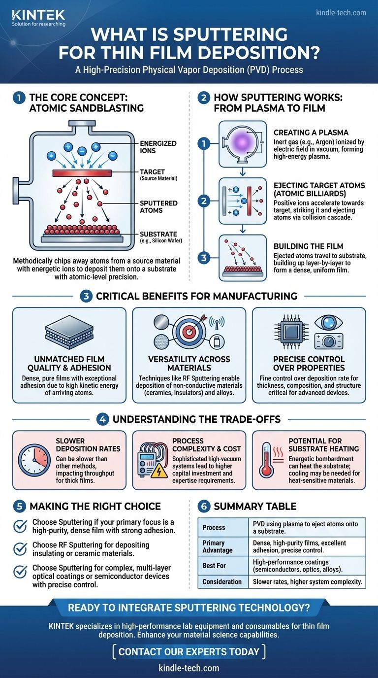
At its core, sputtering is a physical vapor deposition (PVD) process used to create ultra-thin films with atomic-level precision. It works by bombarding a source material, known as a "target," with high-energy ions from a plasma. This collision ejects atoms from the target, which then travel and deposit onto a "substrate," such as a silicon wafer or a glass lens, forming a uniform and tightly bonded coating.
Sputtering is best understood as a form of "atomic sandblasting." It uses energetic ions to methodically chip away atoms from a source material and redeposit them elsewhere, enabling the creation of high-performance films that are fundamental to modern electronics, optics, and advanced materials.
How Sputtering Works: From Plasma to Film
To grasp why sputtering is so versatile, it’s helpful to understand the key steps involved in the process, which all occur within a high-vacuum chamber.
The Core Mechanism: Creating a Plasma
The process begins by introducing a small amount of an inert gas, most commonly Argon, into a vacuum chamber. A strong electric field is applied, which ionizes the gas and creates a plasma—a glowing, high-energy state of matter composed of positive ions and free electrons.
Atomic Billiards: Ejecting Target Atoms
These newly formed positive ions are accelerated by the electric field and directed with great force toward the target, which is made of the material you wish to deposit.
When an ion strikes the target, it transfers its momentum in a "collision cascade." This is much like a cue ball striking a tightly packed rack of billiard balls, causing atoms to be ejected or "sputtered" from the target's surface.
Deposition: Building the Film
The ejected target atoms travel through the vacuum chamber and land on the substrate, which is strategically placed to receive them. Over time, these atoms build up layer-by-layer, forming a thin, dense, and highly uniform film that adheres securely to the substrate surface.
Why Sputtering is a Critical Manufacturing Tool
Sputtering isn't just one method among many; its unique characteristics make it indispensable for high-performance applications where material properties are paramount.
Unmatched Film Quality and Adhesion
Because the sputtered atoms arrive at the substrate with significant kinetic energy, they form exceptionally dense and pure films. This energy also promotes strong adhesion between the film and the substrate, resulting in coatings that are durable and reliable.
Versatility Across Materials
While basic sputtering requires a conductive target, techniques like RF (Radio Frequency) sputtering can be used on non-conductive materials. This opens the door to depositing a vast range of substances, including ceramics, insulators, and complex alloys, not just metals.
Precise Control Over Film Properties
The sputtering process allows for extremely fine control over the deposition rate. This enables engineers to precisely manage the thickness, composition, and structure of the film, which is critical for manufacturing advanced devices like semiconductors and optical filters.
Understanding the Trade-offs
While powerful, sputtering is not a universal solution. Understanding its limitations is key to making an informed decision.
Slower Deposition Rates
Compared to other methods like thermal evaporation, sputtering can be a slower process. This can impact manufacturing throughput and cost, especially for applications requiring very thick films.
Process Complexity and Cost
Sputtering systems are sophisticated pieces of equipment involving high-vacuum chambers, multiple gas lines, high-voltage power supplies, and often, magnetic fields (in magnetron sputtering). This complexity leads to higher initial capital investment and operational expertise.
Potential for Substrate Heating
The constant bombardment of energetic particles can transfer significant heat to the substrate. For heat-sensitive substrates, such as certain plastics or biological materials, this can cause damage if not properly managed with a cooling system.
Making the Right Choice for Your Goal
Sputtering is chosen when the performance and precision of the thin film justify the investment in the process.
- If your primary focus is a high-purity, dense film with strong adhesion: Sputtering is an exceptional choice due to the energetic nature of the deposition process.
- If your primary focus is depositing insulating or ceramic materials: RF sputtering provides the critical capability to work with non-conductive targets, a key advantage over simpler methods.
- If your primary focus is creating complex, multi-layer optical coatings or semiconductor devices: Sputtering offers the atomic-level control over thickness and composition required for these demanding applications.
Ultimately, sputtering empowers engineers to build materials atom-by-atom, making it an indispensable tool for creating next-generation products.
Summary Table:
| Aspect | Key Takeaway |
|---|---|
| Process | Physical Vapor Deposition (PVD) using plasma to eject atoms from a target onto a substrate. |
| Primary Advantage | Creates dense, high-purity films with excellent adhesion and precise control over thickness. |
| Best For | Applications requiring high-performance coatings, like semiconductors, optics, and advanced alloys. |
| Consideration | Slower deposition rates and higher system complexity compared to some other methods. |
Ready to integrate sputtering technology into your lab's workflow?
KINTEK specializes in providing high-performance lab equipment and consumables for thin film deposition. Our expertise ensures you get the right sputtering solutions for your specific research or production needs, from semiconductor fabrication to advanced optical coatings.
Contact our experts today to discuss how our reliable sputtering systems can enhance your material science capabilities and drive your innovations forward.
Visual Guide
Related Products
- Spark Plasma Sintering Furnace SPS Furnace
- Vacuum Induction Melting Spinning System Arc Melting Furnace
- Chemical Vapor Deposition CVD Equipment System Chamber Slide PECVD Tube Furnace with Liquid Gasifier PECVD Machine
- Customer Made Versatile CVD Tube Furnace Chemical Vapor Deposition Chamber System Equipment
People Also Ask
- What is the theory of spark plasma sintering? A Guide to Rapid, Low-Temperature Densification
- What are the advantages of CAMI/SPS for W-Cu composite preparation? Reduce cycles from hours to seconds.
- What technical advantages does a Spark Plasma Sintering (SPS) furnace offer for LZP ceramics? Enhance Ionic Conductivity
- Why are Spark Plasma Sintering (SPS) furnaces or hot presses utilized in the preparation of Li3PS4 solid electrolytes?
- What is SPS sintering method? A Guide to High-Speed, High-Performance Material Fabrication


