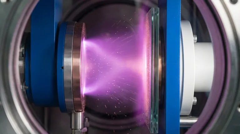
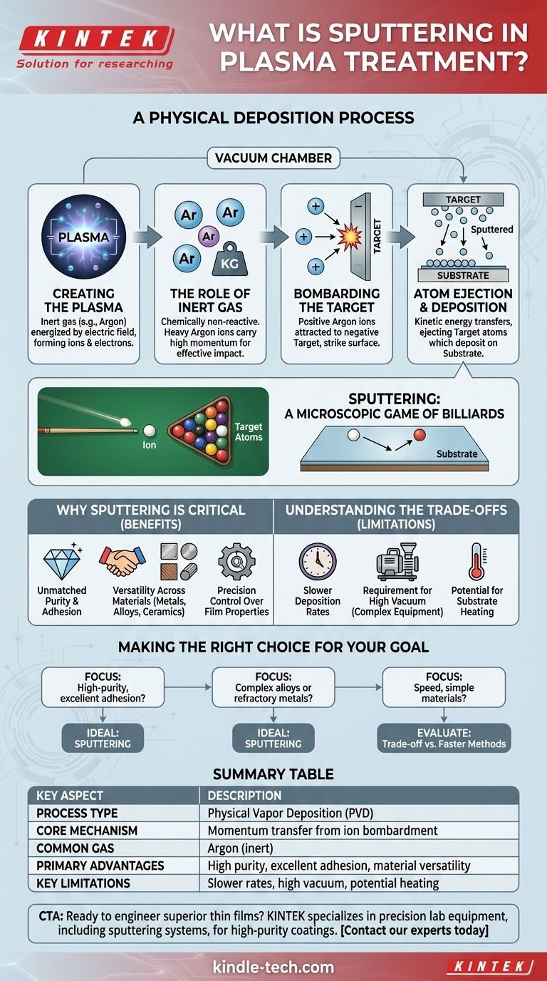
At its core, sputtering is a physical deposition process, not a chemical one. In a high-vacuum environment, a process gas is energized into a plasma. Ions from this plasma are accelerated to bombard a source material, known as the "target," dislodging its atoms which then travel and deposit as a thin, uniform film onto a substrate.
Sputtering is best understood as a microscopic game of billiards. High-energy ions act as the cue ball, striking atoms on a target material and knocking them loose. These ejected atoms then coat another surface, allowing for the precise engineering of high-purity thin films.
The Core Mechanism: From Plasma to Deposition
To understand sputtering, it's essential to break down the distinct steps that occur within the vacuum chamber. The entire process relies on controlled momentum transfer.
Creating the Plasma
The process begins by introducing a small amount of an inert gas, such as argon, into a high-vacuum chamber. An electric field is then applied, which strips electrons from the gas atoms. This creates a mixture of positively charged ions and free electrons, forming the energized state of matter known as plasma.
The Role of the Inert Gas
An inert gas is chosen because it is chemically non-reactive, ensuring the process remains purely physical. Argon is the most common choice for a critical reason: its atomic mass.
Compared to lighter inert gases like helium or neon, the heavier argon ions carry more momentum. This makes them significantly more effective at knocking atoms loose from the target upon impact, improving the efficiency of the process.
Bombarding the Target
The source material to be deposited, the target, is given a negative electrical charge. This attracts the positively charged argon ions from the plasma, causing them to accelerate and collide with the target's surface with significant force.
Atom Ejection and Deposition
Each collision transfers kinetic energy from the argon ion to the target material. If enough energy is transferred, an atom is ejected, or "sputtered," from the target's surface. These ejected atoms travel through the vacuum until they strike the substrate (the material to be coated), gradually building up a thin film layer by layer.
Why Sputtering is a Critical Process
Sputtering is not just one of many options; for certain applications, it provides capabilities that other methods cannot match.
Unmatched Purity and Adhesion
Because the process occurs in a high vacuum and involves no chemical reactions, the resulting films are exceptionally pure. The high energy of the depositing atoms also results in films with superior adhesion to the substrate compared to lower-energy processes like thermal evaporation.
Versatility Across Materials
Sputtering can be used to deposit a vast range of materials, including pure metals, complex alloys, and even insulating ceramic compounds. This makes it a foundational technique in manufacturing semiconductors, optical coatings, and advanced medical devices.
Precision Control Over Film Properties
The process allows for exceptionally fine control over the thickness and uniformity of the deposited film. By carefully managing gas pressure, power, and time, engineers can create films with highly specific and repeatable characteristics.
Understanding the Trade-offs
No technical process is without its limitations. Objectivity requires acknowledging where sputtering may not be the optimal choice.
Slower Deposition Rates
Generally, sputtering is a slower process compared to some chemical vapor deposition (CVD) or thermal evaporation techniques. This can be a limiting factor for applications requiring very thick films or high-volume manufacturing.
Requirement for High Vacuum
The need for a high-vacuum environment necessitates complex and expensive equipment. This includes powerful vacuum pumps and sealed chambers, which increases both the initial capital investment and ongoing maintenance costs.
Potential for Substrate Heating
The constant bombardment of high-energy particles (including ions and ejected atoms) can transfer a significant amount of heat to the substrate. This may damage temperature-sensitive substrates, such as certain plastics or biological materials, unless active cooling is implemented.
Making the Right Choice for Your Goal
Selecting a deposition technique depends entirely on the desired outcome for the final product.
- If your primary focus is high-purity films with excellent adhesion: Sputtering is an ideal choice due to its physical nature and the high kinetic energy of the deposited atoms.
- If your primary focus is depositing complex alloys or refractory metals: Sputtering offers superior control and capability, as it can deposit materials without altering their composition.
- If your primary focus is speed and coating simple materials: You may need to evaluate the trade-off between sputtering's quality and the potentially faster rates of simpler methods like thermal evaporation.
Understanding these core principles allows you to leverage sputtering not just as a process, but as a precise tool for advanced material engineering.
Summary Table:
| Key Aspect | Description |
|---|---|
| Process Type | Physical Vapor Deposition (PVD) |
| Core Mechanism | Momentum transfer from ion bombardment |
| Common Gas | Argon (inert) |
| Primary Advantages | High purity, excellent adhesion, material versatility |
| Key Limitations | Slower deposition rates, requires high vacuum, potential substrate heating |
Ready to engineer superior thin films for your lab?
KINTEK specializes in precision lab equipment, including sputtering systems, to help you achieve high-purity coatings with excellent adhesion for your semiconductor, optical, or medical device projects. Our expertise ensures you get the right solution for your specific material and application requirements.
Contact our experts today to discuss how our sputtering solutions can enhance your research and development.
Visual Guide
Related Products
- Spark Plasma Sintering Furnace SPS Furnace
- Vacuum Induction Melting Spinning System Arc Melting Furnace
- Chemical Vapor Deposition CVD Equipment System Chamber Slide PECVD Tube Furnace with Liquid Gasifier PECVD Machine
- Customer Made Versatile CVD Tube Furnace Chemical Vapor Deposition Chamber System Equipment
- Vacuum Cold Mounting Machine for Sample Preparation
People Also Ask
- What are the fundamentals of spark plasma sintering process? Unlock Rapid, High-Performance Material Consolidation
- What are the advantages of CAMI/SPS for W-Cu composite preparation? Reduce cycles from hours to seconds.
- What is the mechanism of SPS process? A Deep Dive into Rapid, Low-Temperature Sintering
- What is the process fundamentals of spark plasma sintering? Achieve Rapid, High-Density Material Consolidation
- What is the pressure for spark plasma sintering? A Guide to Optimizing SPS Parameters


