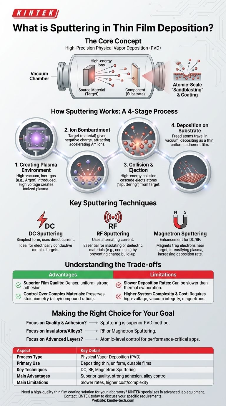
In the world of advanced manufacturing, sputtering is a high-precision coating process classified as a form of physical vapor deposition (PVD). On a fundamental level, it involves ejecting atoms from a source material (called a "target") by bombarding it with high-energy ions inside a vacuum. These dislodged atoms then travel and deposit onto a component (the "substrate"), forming an exceptionally thin, uniform, and durable film.
At its core, sputtering is an atomic-scale "sandblasting" and coating process. It physically knocks atoms off a source material and redeposits them onto a surface, giving engineers precise control over a film's thickness, density, and composition.
How Sputtering Works: A Step-by-Step Breakdown
To understand sputtering, it's best to visualize it as a controlled, four-stage process occurring within a specialized vacuum chamber.
Step 1: Creating the Plasma Environment
The process begins in a high-vacuum chamber, which is backfilled with a small, controlled amount of an inert gas, typically Argon (Ar). A high voltage is then applied, stripping electrons from the argon atoms and creating a glowing, ionized gas known as a plasma.
Step 2: Ion Bombardment of the Target
The target, which is made of the material to be deposited, is given a negative electrical charge. This causes the positively charged argon ions (Ar+) from the plasma to accelerate aggressively and collide with the target's surface.
Step 3: The Collision Cascade and Ejection
When a high-energy ion strikes the target, it transfers its momentum to the target atoms. This sets off a collision cascade beneath the surface, similar to a sub-atomic chain reaction. This cascade ultimately results in atoms from the target's surface being physically knocked loose, or "sputtered."
Step 4: Deposition onto the Substrate
These newly freed atoms from the target travel through the vacuum chamber and land on the substrate (the object being coated, such as a silicon wafer or optical lens). Because they arrive with significant energy, they form a very dense, well-adhered, and highly uniform thin film.
Key Sputtering Techniques
While the principle is the same, different sputtering techniques are used depending on the material and desired outcome.
DC Sputtering
This is the simplest form, where a direct current (DC) voltage is used. It works exceptionally well for depositing electrically conductive metallic targets.
RF Sputtering
For insulating or dielectric materials (like ceramics), a DC current won't work. Radio Frequency (RF) Sputtering uses an alternating current that rapidly switches polarity. This prevents charge build-up on the target, allowing non-conductive materials to be sputtered effectively and dramatically broadening the process's applications.
Magnetron Sputtering
This is an enhancement that can be applied to both DC and RF sputtering. Strong magnets are placed behind the target to trap electrons in the plasma close to its surface. This intensifies the ionization of the argon gas, creating a much denser plasma, which significantly increases the deposition rate and reduces substrate heating.
Understanding the Trade-offs
Sputtering is a powerful technique, but it involves specific advantages and limitations that are critical to understand.
Advantage: Superior Film Quality
Sputtered films are typically much denser, more uniform, and have stronger adhesion to the substrate compared to other methods like thermal evaporation. The higher kinetic energy of the deposited atoms is a key reason for this.
Advantage: Control Over Complex Materials
Sputtering excels at depositing alloys and compound materials. The process faithfully transfers the material from the target to the substrate, preserving the original stoichiometry (the elemental proportions).
Limitation: Slower Deposition Rates
In some cases, especially when compared to simple thermal evaporation, sputtering can be a slower process. Magnetron sputtering was developed specifically to help mitigate this issue by increasing deposition speed.
Limitation: Higher System Complexity and Cost
Sputtering systems, with their need for high-voltage power supplies, vacuum integrity, and (often) magnetrons, are generally more complex and expensive than simpler deposition techniques.
Making the Right Choice for Your Goal
Sputtering is a foundational technology for countless industries, from semiconductors and optics to medical devices and data storage. Applying it correctly depends entirely on the film's required properties.
- If your primary focus is film quality, uniformity, and adhesion: Sputtering is almost always the superior Physical Vapor Deposition method.
- If your primary focus is depositing an insulating material or a complex alloy: RF or Magnetron Sputtering is the definitive choice for maintaining composition and quality.
- If your primary focus is creating advanced optical or electronic layers: Sputtering provides the atomic-level control needed for performance-critical applications like anti-reflective coatings and semiconductor circuits.
By understanding its core mechanism, you can leverage sputtering to engineer materials at the atomic level, enabling the next generation of advanced technology.
Summary Table:
| Aspect | Key Detail |
|---|---|
| Process Type | Physical Vapor Deposition (PVD) |
| Primary Use | Depositing thin, uniform, and durable films |
| Key Techniques | DC Sputtering, RF Sputtering, Magnetron Sputtering |
| Main Advantages | Superior film quality, strong adhesion, excellent control for alloys and compounds |
| Main Limitations | Slower deposition rates, higher system complexity and cost |
Need a high-quality thin film coating solution for your laboratory?
Sputtering is the definitive choice for applications requiring superior film density, uniformity, and adhesion—from semiconductor wafers and optical lenses to medical devices. KINTEK specializes in providing advanced lab equipment and consumables, including sputtering systems, to meet your precise research and production needs.
Let our experts help you achieve atomic-level control for your next project. Contact KINTEK today to discuss your specific requirements and discover the right sputtering solution for your laboratory.
Visual Guide
Related Products
- Spark Plasma Sintering Furnace SPS Furnace
- Vacuum Induction Melting Spinning System Arc Melting Furnace
- Chemical Vapor Deposition CVD Equipment System Chamber Slide PECVD Tube Furnace with Liquid Gasifier PECVD Machine
- Customer Made Versatile CVD Tube Furnace Chemical Vapor Deposition Chamber System Equipment
- Vacuum Cold Mounting Machine for Sample Preparation
People Also Ask
- What is the theory of spark plasma sintering? A Guide to Rapid, Low-Temperature Densification
- What are the advantages of CAMI/SPS for W-Cu composite preparation? Reduce cycles from hours to seconds.
- Why are Spark Plasma Sintering (SPS) furnaces or hot presses utilized in the preparation of Li3PS4 solid electrolytes?
- What is the mechanism of SPS process? A Deep Dive into Rapid, Low-Temperature Sintering
- What is the difference between spark plasma sintering and flash sintering? A Guide to Advanced Sintering Methods


