Sputtering is a highly controlled Physical Vapor Deposition (PVD) process used to create exceptionally thin, high-quality films. In essence, it converts a solid source material directly into a vapor not by melting it, but by bombarding it with high-energy ions in a vacuum. These dislodged atoms then travel and deposit onto a substrate, forming a precise and uniform coating.
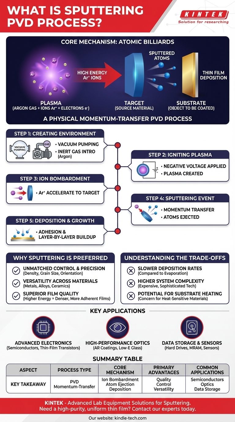
The critical concept to understand is that sputtering is not a thermal process; it is a physical momentum-transfer process. Think of it as a game of atomic billiards, where energetic gas ions are the cue ball, striking a target material and ejecting its atoms, which then form a pristine film on a nearby surface.
The Core Mechanism: From Plasma to Thin Film
To understand sputtering, it's best to visualize the sequence of events that occur within the vacuum chamber. Each step is precisely controlled to achieve the desired film characteristics.
Step 1: Creating the Environment
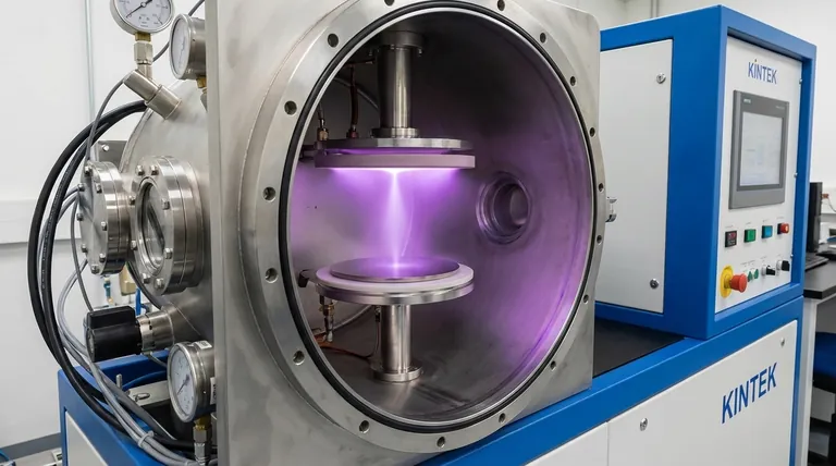
The entire process begins by placing the source material, called the target, and the object to be coated, the substrate, into a vacuum chamber. The chamber is pumped down to a very low pressure to remove contaminants. Then, a small, controlled amount of an inert gas, most commonly Argon, is introduced.
Step 2: Igniting the Plasma
A high negative voltage is applied to the target, causing it to become a cathode. This strong electric field causes free electrons to accelerate and collide with the neutral Argon gas atoms. These collisions knock electrons off the Argon atoms, creating a glowing, ionized gas known as plasma.
Step 3: Ion Bombardment
Within the plasma, you now have positively charged Argon ions (Ar+) and free electrons. The powerful negative charge of the target aggressively attracts these positive Argon ions. They accelerate towards the target at extremely high velocity.
Step 4: The Sputtering Event
The high-energy Argon ions slam into the surface of the target material. This collision is a pure momentum transfer. The impact has enough kinetic energy to dislodge, or "sputter," individual atoms or molecules from the target material, sending them flying into the vacuum chamber.
Step 5: Deposition and Film Growth
These sputtered atoms travel in a straight line until they strike the substrate. Upon arrival, they stick to the surface, a process called adhesion, and gradually build up, layer by atomic layer, to form a dense, uniform, and highly pure thin film.
Why Sputtering Is a Preferred Method
Sputtering is chosen for demanding applications because the process itself provides unique advantages over other deposition techniques.
Unmatched Control and Precision
Because it is a physical, not a thermal, process, sputtering allows for exquisite control over the final film. Engineers can precisely manipulate film properties like density, grain size, orientation, and electrical resistivity by adjusting process parameters like gas pressure and voltage.
Versatility Across Materials
Sputtering can deposit a vast range of materials, including metals, alloys, and even insulating ceramic compounds that would be difficult or impossible to deposit using thermal evaporation. The composition of the sputtered film is typically identical to the composition of the source target.
Superior Film Quality
The sputtered atoms arrive at the substrate with significantly more kinetic energy than evaporated atoms. This higher energy promotes better surface mobility and results in films that are denser, more adherent, and more uniform.
Understanding the Trade-offs
No process is perfect, and sputtering is chosen when its benefits outweigh its inherent limitations. Understanding these trade-offs is key to making an informed decision.
Slower Deposition Rates
Generally, sputtering is a slower process compared to thermal evaporation. For applications where thick films are needed quickly and precision is less critical, sputtering may not be the most efficient choice.
Higher System Complexity
Sputtering systems are more complex and expensive than simple evaporation systems. They require sophisticated high-voltage power supplies, precise gas flow control, and robust vacuum technology to operate effectively.
Potential for Substrate Heating
The constant bombardment of energetic particles, including sputtered atoms and neutral gas atoms, can transfer a significant amount of energy to the substrate, causing it to heat up. This can be a concern when coating temperature-sensitive materials like plastics.
Key Applications for Sputtering
The unique capabilities of sputtering make it the go-to process for many of today's most advanced technologies.
- If your primary focus is advanced electronics: Sputtering provides the ultra-pure, uniform conductive and dielectric layers required for semiconductor circuits and thin-film transistors.
- If your primary focus is high-performance optics: It is the ideal method for creating the complex, multi-layer anti-reflective (AR) coatings for eyeglasses and low-emissivity (low-E) coatings for architectural glass.
- If your primary focus is data storage and sensors: The precise magnetic and resistive films needed for hard drives, MRAM, and various sensor types are almost exclusively deposited via sputtering.
Ultimately, sputtering is the definitive choice when the precision, purity, and structural quality of a thin film are paramount to the performance of the final product.
Summary Table:
| Aspect | Key Takeaway |
|---|---|
| Process Type | Physical Vapor Deposition (PVD), a momentum-transfer (non-thermal) process. |
| Core Mechanism | Energetic ions bombard a target, ejecting atoms that deposit as a thin film on a substrate. |
| Primary Advantages | Superior film quality, excellent control, versatility with metals/ceramics, high purity. |
| Common Applications | Semiconductor devices, optical coatings, data storage media, and various sensors. |
Need a high-purity, uniform thin film for your application?
KINTEK specializes in advanced lab equipment, including sputtering systems, to meet the demanding needs of R&D and production laboratories. Whether you are developing next-generation semiconductors, precision optics, or advanced sensors, our expertise ensures you achieve the precise film properties required for success.
Contact our experts today to discuss how our sputtering solutions can enhance your research and manufacturing processes.
Visual Guide
Related Products
- RF PECVD System Radio Frequency Plasma-Enhanced Chemical Vapor Deposition RF PECVD
- Inclined Rotary Plasma Enhanced Chemical Vapor Deposition PECVD Equipment Tube Furnace Machine
- Chemical Vapor Deposition CVD Equipment System Chamber Slide PECVD Tube Furnace with Liquid Gasifier PECVD Machine
- Electron Beam Evaporation Coating Oxygen-Free Copper Crucible and Evaporation Boat
- Customer Made Versatile CVD Tube Furnace Chemical Vapor Deposition Chamber System Equipment
People Also Ask
- What is plasma activated chemical vapour deposition method? A Low-Temperature Solution for Advanced Coatings
- Why does PECVD commonly use RF power input? For Precise Low-Temperature Thin Film Deposition
- How are PECVD and CVD different? A Guide to Choosing the Right Thin-Film Deposition Process
- What is the principle of plasma enhanced chemical vapor deposition? Achieve Low-Temperature Thin Film Deposition
- Why is PECVD environment friendly? Understanding the Eco-Friendly Benefits of Plasma-Enhanced Coating