The fundamental advantage of magnetron sputtering is its ability to produce high-quality, dense, and strongly adhered thin films at high deposition rates. It achieves this by using a magnetic field to create a highly efficient plasma, a process that works on a vast range of materials, including those with very high melting points that cannot be easily evaporated.
Magnetron sputtering should not be seen as just one of many coating methods. It is a highly controllable and scalable platform technology that leverages magnetic fields to overcome the core limitations of conventional sputtering, enabling faster, cooler, and more efficient deposition for demanding industrial and research applications.
How Magnetic Fields Revolutionize the Sputtering Process
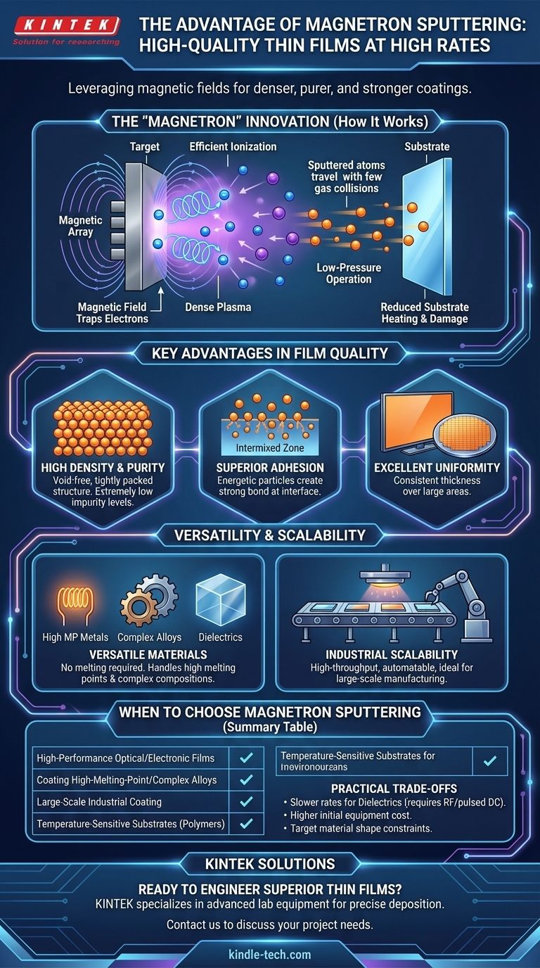
The "magnetron" in the name is the key innovation. A magnetic field is strategically placed behind the material to be deposited (the "target"), which dramatically improves the process.
Trapping Electrons for Efficient Ionization
In any sputtering process, inert gas ions (like Argon) are accelerated to strike a target, knocking off atoms that then deposit on your substrate.
Magnetron sputtering uses a magnetic field to trap electrons near the target surface. These trapped electrons travel a much longer, spiral path, drastically increasing the probability they will collide with and ionize neutral argon atoms.
This creates a dense, stable plasma precisely where it's needed, leading to a much more efficient sputtering of the target material.
Enabling Low-Pressure and Low-Damage Deposition
Because the plasma is so efficiently generated and confined, the entire process can operate at much lower pressures and voltages.
This has two critical benefits. First, lower pressure means the sputtered atoms travel to the substrate with fewer gas-phase collisions, retaining more energy for better film quality. Second, it significantly reduces electron bombardment and heating of the substrate, preventing damage to sensitive materials.
Key Advantages in Film Quality and Performance
The unique physics of the magnetron process translates directly into superior film characteristics that are difficult to achieve with other methods.
Achieving High Film Density and Purity
Atoms ejected from the target in magnetron sputtering have higher kinetic energy than those from simple thermal evaporation.
When these energetic atoms arrive at the substrate, they arrange themselves into a tightly packed, dense film with very few voids. The high-vacuum environment also ensures extremely low levels of impurities are incorporated into the film.
Ensuring Superior Adhesion
The higher energy of the depositing particles also allows them to slightly implant into the substrate's surface.
This creates an "intermixed" zone at the interface, which results in exceptionally strong adhesion between the film and the substrate. This is critical for films that must withstand wear, stress, or thermal cycling.
Delivering Excellent Uniformity Over Large Areas
The process is remarkably stable and controllable, allowing for the deposition of films with highly uniform thickness and composition across very large areas.
This makes it the go-to technology for manufacturing applications like architectural glass, flat-panel displays, and semiconductor wafers, where consistency is paramount.
Versatility and Industrial Scalability
Beyond film quality, magnetron sputtering offers unmatched flexibility and is perfectly suited for high-volume production.
Sputtering Difficult and Complex Materials
Because magnetron sputtering is a physical, not a thermal, process, it does not require melting the source material.
This allows it to deposit materials with extremely high melting points (like tungsten or tantalum), complex alloys (which deposit with their original composition intact), and even dielectric compounds.
Protecting Heat-Sensitive Substrates
The lower substrate heating mentioned earlier is a crucial advantage. It enables high-quality coatings to be applied to temperature-sensitive materials like plastics, polymers, and even paper without causing them to melt or deform.
Designed for High-Throughput Manufacturing
The combination of high deposition rates for metals, excellent large-area uniformity, and suitability for automation makes magnetron sputtering ideal for industrial-scale production. It is a repeatable and reliable process that can be scaled up to meet high-throughput demands.
Understanding the Practical Trade-offs
While powerful, magnetron sputtering is not without its considerations. Objectivity requires acknowledging where it may be less suitable.
Slower Deposition Rates for Dielectrics
While deposition rates for metals are very high, sputtering insulating materials (dielectrics) is more complex. It requires a Radio Frequency (RF) or pulsed DC power supply, which typically results in significantly lower deposition rates compared to conductive materials.
Higher Initial Equipment Cost
The necessary equipment—including vacuum chambers, high-voltage power supplies, and specialized magnetic targets—is more complex and carries a higher initial investment cost compared to simpler techniques like thermal evaporation.
Target Material Constraints
The source material must be fabricated into a specific shape and size to serve as a sputtering target. This can sometimes be challenging or costly for rare, brittle, or difficult-to-machine materials.
When to Choose Magnetron Sputtering
Your choice of deposition technology should always be driven by the specific requirements of your final product.
- If your primary focus is high-performance optical or electronic films: The superior purity, density, and uniformity make magnetron sputtering the ideal choice.
- If your primary focus is coating high-melting-point metals or complex alloys: Magnetron sputtering is one of the few methods that can handle these materials while preserving their composition.
- If your primary focus is large-scale industrial coating: Its scalability, high rate for metals, and potential for automation provide unmatched throughput and repeatability.
- If your primary focus is coating temperature-sensitive substrates like polymers: The low-temperature nature of the process protects the substrate from thermal damage.
Ultimately, magnetron sputtering provides a uniquely powerful combination of control, quality, and scalability for engineering advanced thin films.
Summary Table:
| Key Advantage | Description |
|---|---|
| High Film Density & Purity | Produces tightly packed, void-free films with minimal impurities in a high-vacuum environment. |
| Superior Adhesion | Energetic particles create an intermixed zone at the interface for strong film-substrate bonding. |
| Excellent Uniformity | Ensures consistent thickness and composition across large areas like wafers or display panels. |
| Versatility with Materials | Handles high-melting-point metals, alloys, and dielectrics without thermal damage to substrates. |
| Low-Temperature Deposition | Protects heat-sensitive substrates (e.g., plastics) by operating at lower pressures and voltages. |
Ready to Engineer Superior Thin Films with Magnetron Sputtering?
At KINTEK, we specialize in providing advanced lab equipment and consumables for precise thin film deposition. Whether you're in research or high-volume manufacturing, our magnetron sputtering solutions deliver the density, adhesion, and uniformity your projects demand.
Contact us today to discuss how our expertise can enhance your laboratory's capabilities and accelerate your innovation.
Visual Guide
Related Products
- Spark Plasma Sintering Furnace SPS Furnace
- RF PECVD System Radio Frequency Plasma-Enhanced Chemical Vapor Deposition RF PECVD
People Also Ask
- What is SPS sintering method? A Guide to High-Speed, High-Performance Material Fabrication
- What is the pressure for spark plasma sintering? A Guide to Optimizing SPS Parameters
- What are the advantages of CAMI/SPS for W-Cu composite preparation? Reduce cycles from hours to seconds.
- What is the process fundamentals of spark plasma sintering? Achieve Rapid, High-Density Material Consolidation
- What is the mechanism of SPS process? A Deep Dive into Rapid, Low-Temperature Sintering

