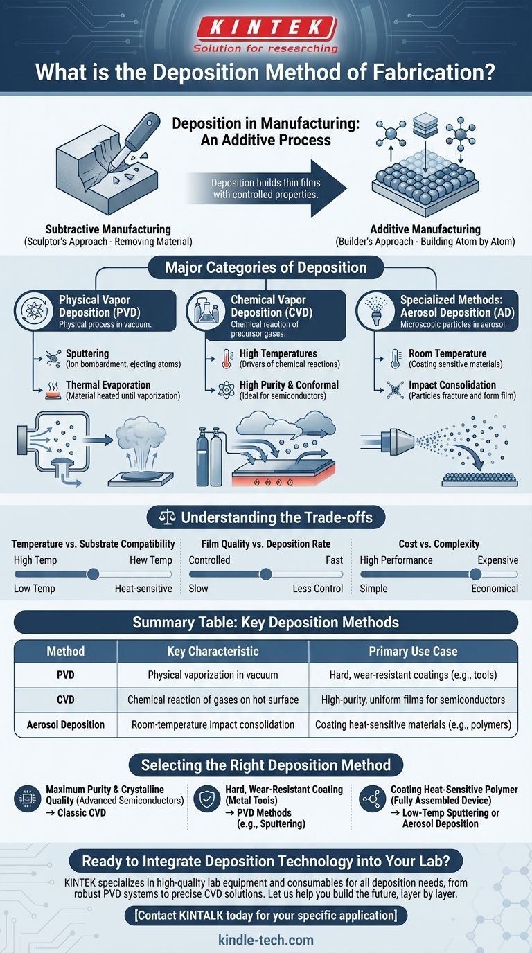
In manufacturing, deposition is the process of applying a thin film of material onto a surface, known as a substrate. This method is fundamental to modern technology, serving as the primary way we build complex structures in semiconductors, optics, and advanced materials. Unlike carving or cutting material away, deposition is an additive process that builds objects atom by atom or layer by layer.
Deposition is not a single technique but a family of processes used to build things from the ground up. The core challenge is controlling how atoms or molecules land on a surface to create a film with specific, desired properties.
Additive vs. Subtractive Manufacturing
To understand deposition, it's useful to contrast it with the more traditional manufacturing approach.
Subtractive Manufacturing: The Sculptor's Approach
Subtractive manufacturing starts with a larger block of material and removes unwanted parts. Think of a sculptor carving a statue from marble or a machinist milling a metal part. Etching processes in chip manufacturing also fall into this category.
Additive Manufacturing: The Builder's Approach
Deposition is a form of additive manufacturing. It starts with nothing on the substrate and systematically adds material to create the final structure. This bottom-up approach allows for the creation of extremely thin, complex, and highly controlled layers, which is impossible with subtractive methods.
Major Categories of Deposition
The specific technique used depends on the material being deposited and the required characteristics of the final film, such as purity, thickness, and structure. The main families are Physical and Chemical Vapor Deposition.
Physical Vapor Deposition (PVD)
In PVD, a material is converted into a vapor through purely physical means and then transported to the substrate, where it condenses back into a solid film.
This is typically done in a vacuum. Common methods include sputtering, where a target is bombarded with high-energy ions to eject atoms, and thermal evaporation, where a material is heated until it vaporizes.
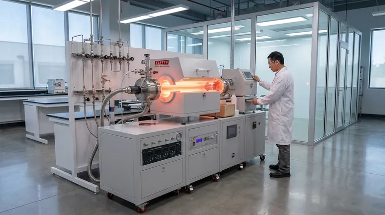
Chemical Vapor Deposition (CVD)
In CVD, the substrate is exposed to one or more volatile precursor gases. These gases react or decompose on the substrate's surface to produce the desired solid film.
CVD often requires high temperatures to drive the chemical reactions. It is prized in the semiconductor industry for its ability to create extremely high-purity and uniform films that conform perfectly to complex surface topologies.
Specialized Methods: Aerosol Deposition
Newer, more specialized techniques are constantly being developed to solve specific problems. Aerosol Deposition (AD) is one such method.
In AD, microscopic particles are mixed into a gas to form an aerosol, which is then accelerated through a nozzle toward the substrate. Upon impact, the particles fracture and form a dense, solid film.
The key advantage, as noted in advanced research, is that this can be done at room temperature. This opens the door to coating sensitive materials like polymers or pre-built electronic components that would be damaged by the high heat of traditional CVD.
Understanding the Trade-offs
No single deposition method is perfect for every application. The choice always involves balancing competing requirements.
Temperature vs. Substrate Compatibility
High-temperature processes like CVD can produce excellent film quality but are incompatible with substrates that have low melting points, such as plastics. Low-temperature methods like PVD or Aerosol Deposition are essential for these heat-sensitive applications.
Film Quality vs. Deposition Rate
Some methods, like thermal evaporation, are fast and relatively simple but offer less control over the film's structure and properties. Techniques like Atomic Layer Deposition (a variant of CVD) provide ultimate, single-atom-layer control but are significantly slower and more expensive.
Cost vs. Complexity
The equipment required for deposition can range from moderately complex to exceptionally expensive. The choice often depends on balancing the need for pristine, high-performance films against the economic realities of the product being manufactured.
Selecting the Right Deposition Method
Your choice of deposition technique should be driven directly by the primary goal of your application.
- If your primary focus is maximum purity and crystalline quality for advanced semiconductors: Classic Chemical Vapor Deposition (CVD) is the industry standard.
- If your primary focus is applying a hard, wear-resistant coating onto metal tools: Physical Vapor Deposition (PVD) methods like sputtering are the most effective and widely used.
- If your primary focus is coating a heat-sensitive polymer or a fully assembled device: A low-temperature process like sputtering or an innovative room-temperature method like Aerosol Deposition is necessary.
Ultimately, deposition is the foundational toolkit for building the invisible, high-performance structures that power our modern world.
Summary Table:
| Method | Key Characteristic | Primary Use Case |
|---|---|---|
| Physical Vapor Deposition (PVD) | Physical vaporization in a vacuum | Hard, wear-resistant coatings (e.g., on tools) |
| Chemical Vapor Deposition (CVD) | Chemical reaction of gases on a hot surface | High-purity, uniform films for semiconductors |
| Aerosol Deposition (AD) | Room-temperature impact consolidation | Coating heat-sensitive materials (e.g., polymers) |
Ready to Integrate Deposition Technology into Your Lab?
Choosing the right deposition method is critical for your research and production outcomes. KINTEK specializes in providing high-quality lab equipment and consumables for all your deposition needs, from robust PVD systems to precise CVD solutions.
Our experts can help you select the ideal equipment to achieve the film purity, thickness, and structure your projects demand. Let us help you build the future, layer by layer.
Contact KINTALK today to discuss your specific application and find the perfect deposition solution.
Visual Guide
Related Products
- HFCVD Machine System Equipment for Drawing Die Nano-Diamond Coating
- RF PECVD System Radio Frequency Plasma-Enhanced Chemical Vapor Deposition RF PECVD
- Chemical Vapor Deposition CVD Equipment System Chamber Slide PECVD Tube Furnace with Liquid Gasifier PECVD Machine
- Electron Beam Evaporation Coating Oxygen-Free Copper Crucible and Evaporation Boat
- Hemispherical Bottom Tungsten Molybdenum Evaporation Boat
People Also Ask
- What is the chemical vapor deposition growth process? Build Superior Thin Films from the Atom Up
- What types of substrates are used in CVD to facilitate graphene films? Optimize Graphene Growth with the Right Catalyst
- What is the specific function of the metal filament in HF-CVD? Key Roles in Diamond Growth
- What are the disadvantages and challenges of the HFCVD method? Overcome Growth Limits and Filament Issues
- What are the advantages of chemical vapor deposition? Achieve Superior Thin Films for Your Lab


