Knowledge evaporation boat What is the deposition of thin films? A Guide to Coating Technology for Modern Devices
Author avatar

Tech Team · Kintek Solution

Updated 2 months ago

What is the deposition of thin films? A Guide to Coating Technology for Modern Devices


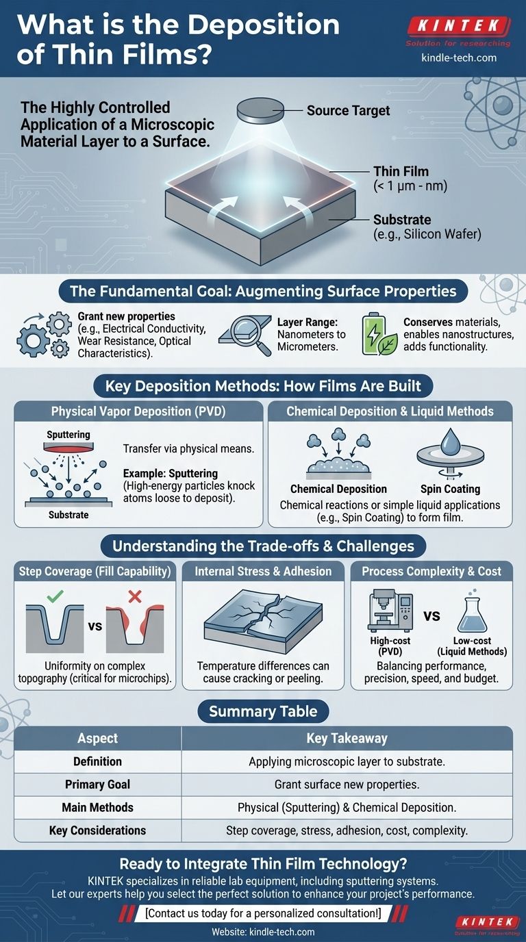
At its core, thin film deposition is the highly controlled process of applying a microscopic layer of one material onto the surface of another, known as a substrate. This synthesis allows us to grant an object's surface new properties—such as electrical conductivity, wear resistance, or specific optical characteristics—that the underlying bulk material does not possess on its own.

Thin film deposition isn't just about applying a coating; it's a foundational manufacturing process for virtually all modern technology. By precisely controlling the application of atomic-scale layers, we can engineer materials with novel properties, enabling everything from powerful microchips to efficient solar panels.

What is the deposition of thin films? A Guide to Coating Technology for Modern Devices

The Fundamental Goal: Augmenting a Material's Surface

What Constitutes a "Thin Film"?

A thin film is a layer of material ranging from fractions of a nanometer to several micrometers in thickness. These layers are so thin that their properties can differ significantly from those of the same material in bulk form.

The Substrate and the Target

The process involves two main components. The substrate is the base material or object being coated, such as a silicon wafer or a piece of glass. The target is the source material that will form the film itself.

Why Not Just Use a Solid Block of Material?

Deposition is used because it provides unique advantages. It conserves rare or expensive materials, allows for the creation of unique nanostructured coatings, and adds functionality with minimal volume and weight.

Key Deposition Methods: How Films Are Built

There are numerous techniques for depositing thin films, which generally fall into two major categories: physical and chemical.

Physical Vapor Deposition (PVD)

PVD techniques transfer material from a solid target to the substrate through physical means.

A common example is sputtering. Imagine a microscopic sandblaster, but instead of eroding a surface, you are using high-energy particles (ions) to bombard a target. This bombardment knocks atoms loose from the target, which then travel and deposit onto the substrate, forming a thin, uniform film.

Chemical Deposition

These methods use chemical reactions at the substrate's surface to form the film. The precursors are often gases or liquids that react or decompose, leaving the desired material behind.

Simpler Liquid-Based Methods

For some applications, simpler methods are sufficient. Techniques like spin coating or drop casting involve applying a liquid precursor and then evaporating the solvent to leave the thin film.

Understanding the Trade-offs

Choosing a deposition method involves balancing performance, cost, and the specific requirements of the final product. No single method is perfect for every application.

The Challenge of Step Coverage

Step coverage, or fill capability, describes how uniformly a film covers a substrate with complex surface topography, like the trenches in a microchip.

It is a critical parameter in semiconductor manufacturing. A process with poor step coverage may create thin, weak spots or gaps in the film, leading to device failure.

Internal Stress and Adhesion

The temperature of the substrate during deposition is a critical factor. Differences in the thermal expansion coefficients between the film and the substrate can create significant internal stress as the component cools.

High stress can cause the film to crack or peel away from the substrate, compromising the device. Managing this stress is key to creating durable and reliable coatings.

Process Complexity and Cost

High-precision methods like sputtering produce excellent, dense films but require expensive vacuum equipment and are relatively slow. Simpler methods like spin coating are fast and cheap but offer less control over the film's final properties.

Making the Right Choice for Your Goal

The best deposition technique depends entirely on your project's technical requirements, material constraints, and budget.

  • If your primary focus is high-purity, dense films for complex electronics: You will likely need a Physical Vapor Deposition method like sputtering for its precise control over thickness and uniformity.
  • If your primary focus is large-area coverage for applications like solar cells or displays: A combination of PVD and chemical methods is often used to balance performance and manufacturing throughput.
  • If your primary focus is rapid prototyping or lab-scale research on a limited budget: Simpler liquid-based methods like spin coating or drop casting offer a viable and accessible starting point.

Understanding these fundamental principles empowers you to select and optimize the processes that turn raw materials into functional, high-performance devices.

Summary Table:

Aspect Key Takeaway
Definition Applying a microscopic layer (nanometers to micrometers) of material onto a substrate.
Primary Goal To grant a surface new properties (e.g., conductivity, hardness) that the bulk material lacks.
Main Methods Physical Vapor Deposition (PVD) like sputtering, and Chemical Deposition.
Key Considerations Step coverage, internal stress, adhesion, process complexity, and cost.

Ready to integrate thin film technology into your research or production?

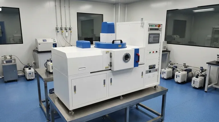
The right deposition equipment is critical for achieving the desired film properties, whether for microchips, solar panels, or advanced coatings. KINTEK specializes in lab equipment and consumables, serving laboratory needs with reliable sputtering systems and more.

Let our experts help you select the perfect solution to enhance your project's performance and efficiency. Contact us today for a personalized consultation!

Visual Guide

What is the deposition of thin films? A Guide to Coating Technology for Modern Devices Visual Guide

Related Products

People Also Ask

Related Products

Aluminized Ceramic Evaporation Boat for Thin Film Deposition

Aluminized Ceramic Evaporation Boat for Thin Film Deposition

Vessel for depositing thin films; has an aluminum-coated ceramic body for improved thermal efficiency and chemical resistance. making it suitable for various applications.

Tungsten Evaporation Boat for Thin Film Deposition

Tungsten Evaporation Boat for Thin Film Deposition

Learn about tungsten boats, also known as evaporated or coated tungsten boats. With a high tungsten content of 99.95%, these boats are ideal for high-temperature environments and widely used in various industries. Discover their properties and applications here.

Electron Beam Evaporation Coating Oxygen-Free Copper Crucible and Evaporation Boat

Electron Beam Evaporation Coating Oxygen-Free Copper Crucible and Evaporation Boat

Electron Beam Evaporation Coating Oxygen-Free Copper Crucible enables precise co-deposition of various materials. Its controlled temperature and water-cooled design ensure pure and efficient thin film deposition.

Molybdenum Tungsten Tantalum Evaporation Boat for High Temperature Applications

Molybdenum Tungsten Tantalum Evaporation Boat for High Temperature Applications

Evaporation boat sources are used in thermal evaporation systems and are suitable for depositing various metals, alloys and materials. Evaporation boat sources are available in different thicknesses of tungsten, tantalum and molybdenum to ensure compatibility with a variety of power sources. As a container, it is used for vacuum evaporation of materials. They can be used for thin film deposition of various materials, or designed to be compatible with techniques such as electron beam fabrication.

Vacuum Hot Press Furnace Machine for Lamination and Heating

Vacuum Hot Press Furnace Machine for Lamination and Heating

Experience clean and precise lamination with Vacuum Lamination Press. Perfect for wafer bonding, thin-film transformations, and LCP lamination. Order now!

HFCVD Machine System Equipment for Drawing Die Nano-Diamond Coating

HFCVD Machine System Equipment for Drawing Die Nano-Diamond Coating

The nano-diamond composite coating drawing die uses cemented carbide (WC-Co) as the substrate, and uses the chemical vapor phase method ( CVD method for short ) to coat the conventional diamond and nano-diamond composite coating on the surface of the inner hole of the mold.

Chemical Vapor Deposition CVD Equipment System Chamber Slide PECVD Tube Furnace with Liquid Gasifier PECVD Machine

Chemical Vapor Deposition CVD Equipment System Chamber Slide PECVD Tube Furnace with Liquid Gasifier PECVD Machine

KT-PE12 Slide PECVD System: Wide power range, programmable temp control, fast heating/cooling with sliding system, MFC mass flow control & vacuum pump.

Inclined Rotary Plasma Enhanced Chemical Vapor Deposition PECVD Equipment Tube Furnace Machine

Inclined Rotary Plasma Enhanced Chemical Vapor Deposition PECVD Equipment Tube Furnace Machine

Introducing our inclined rotary PECVD furnace for precise thin film deposition. Enjoy automatic matching source, PID programmable temperature control, and high accuracy MFC mass flowmeter control. Built-in safety features for peace of mind.

Inclined Rotary Plasma Enhanced Chemical Vapor Deposition PECVD Equipment Tube Furnace Machine

Inclined Rotary Plasma Enhanced Chemical Vapor Deposition PECVD Equipment Tube Furnace Machine

Upgrade your coating process with PECVD coating equipment. Ideal for LED, power semiconductors, MEMS and more. Deposits high-quality solid films at low temps.

Hemispherical Bottom Tungsten Molybdenum Evaporation Boat

Hemispherical Bottom Tungsten Molybdenum Evaporation Boat

Used for gold plating, silver plating, platinum, palladium, suitable for a small amount of thin film materials. Reduce the waste of film materials and reduce heat dissipation.

Customer Made Versatile CVD Tube Furnace Chemical Vapor Deposition Chamber System Equipment

Customer Made Versatile CVD Tube Furnace Chemical Vapor Deposition Chamber System Equipment

Get your exclusive CVD furnace with KT-CTF16 Customer Made Versatile Furnace. Customizable sliding, rotating, and tilting functions for precise reactions. Order now!

Microwave Plasma Chemical Vapor Deposition MPCVD Machine System Reactor for Lab and Diamond Growth

Microwave Plasma Chemical Vapor Deposition MPCVD Machine System Reactor for Lab and Diamond Growth

Get high-quality diamond films with our Bell-jar Resonator MPCVD machine designed for lab and diamond growth. Discover how Microwave Plasma Chemical Vapor Deposition works for growing diamonds using carbon gas and plasma.

Lab Plastic PVC Calender Stretch Film Casting Machine for Film Testing

Lab Plastic PVC Calender Stretch Film Casting Machine for Film Testing

The cast film machine is designed for the molding of polymer cast film products and has multiple processing functions such as casting, extrusion, stretching, and compounding.

915MHz MPCVD Diamond Machine Microwave Plasma Chemical Vapor Deposition System Reactor

915MHz MPCVD Diamond Machine Microwave Plasma Chemical Vapor Deposition System Reactor

915MHz MPCVD Diamond Machine and its multi-crystal effective growth, the maximum area can reach 8 inches, the maximum effective growth area of single crystal can reach 5 inches. This equipment is mainly used for the production of large-size polycrystalline diamond films, the growth of long single crystal diamonds, the low-temperature growth of high-quality graphene, and other materials that require energy provided by microwave plasma for growth.

Small Lab Rubber Calendering Machine

Small Lab Rubber Calendering Machine

Small lab rubber calendering machine is used for producing thin, continuous sheets of plastic or rubber materials. It is commonly employed in laboratories, small-scale production facilities, and prototyping environments to create films, coatings, and laminates with precise thickness and surface finish.

RF PECVD System Radio Frequency Plasma-Enhanced Chemical Vapor Deposition RF PECVD

RF PECVD System Radio Frequency Plasma-Enhanced Chemical Vapor Deposition RF PECVD

RF-PECVD is an acronym for "Radio Frequency Plasma-Enhanced Chemical Vapor Deposition." It deposits DLC (Diamond-like carbon film) on germanium and silicon substrates. It is utilized in the 3-12um infrared wavelength range.

CVD Diamond Dressing Tools for Precision Applications

CVD Diamond Dressing Tools for Precision Applications

Experience the Unbeatable Performance of CVD Diamond Dresser Blanks: High Thermal Conductivity, Exceptional Wear Resistance, and Orientation Independence.

Custom CVD Diamond Coating for Lab Applications

Custom CVD Diamond Coating for Lab Applications

CVD Diamond Coating: Superior Thermal Conductivity, Crystal Quality, and Adhesion for Cutting Tools, Friction, and Acoustic Applications

Single Punch Manual Tablet Press Machine TDP Tablet Punching Machine

Single Punch Manual Tablet Press Machine TDP Tablet Punching Machine

Single punch manual tablet punching machine can press various granular, crystal or powdery raw materials with good fluidity into disc-shaped, cylindrical, spherical, convex, concave and other various geometric shapes (such as square, triangle, ellipse, capsule shape, etc.), and can also press products with text and patterns.


Leave Your Message