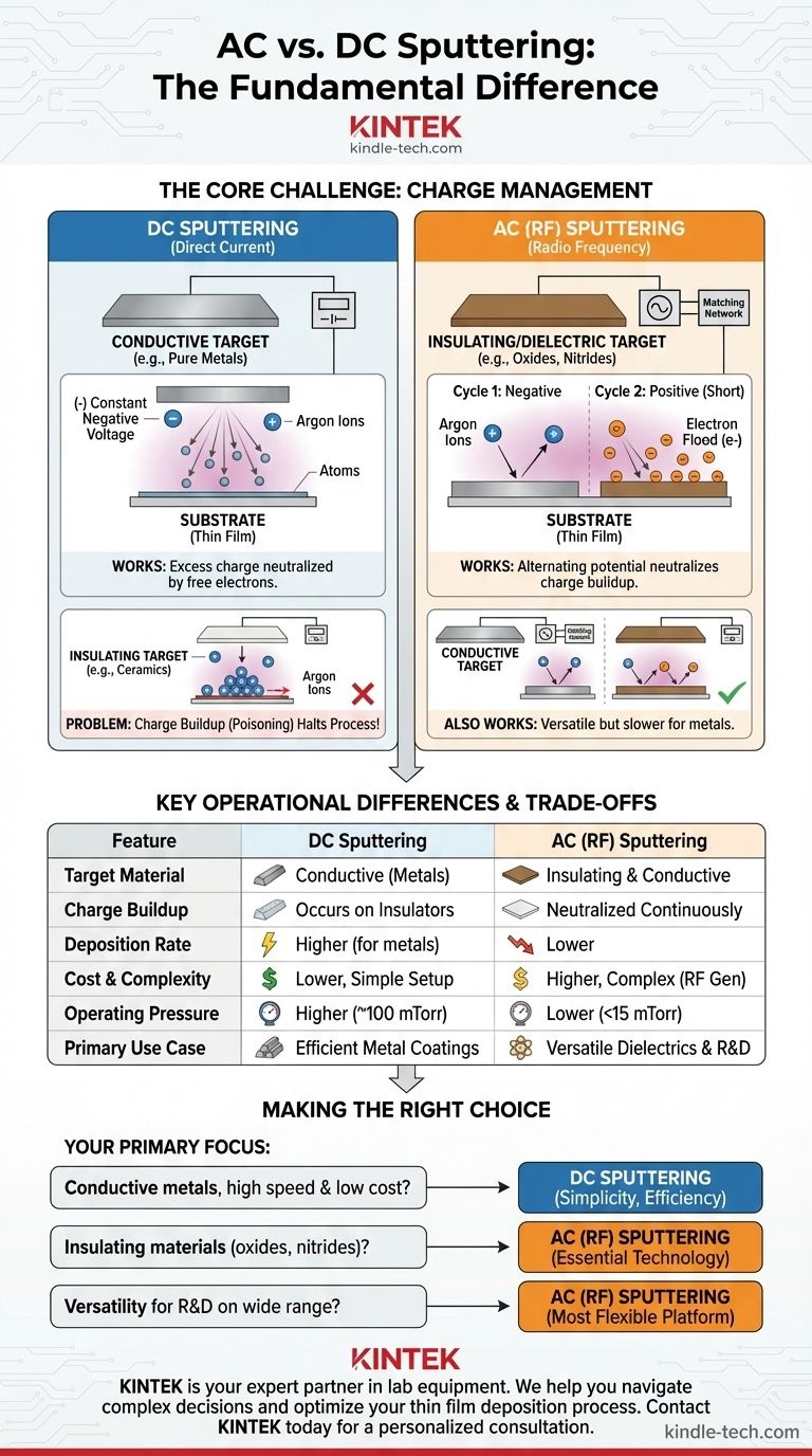
The fundamental difference between AC and DC sputtering lies in the type of material they can deposit. DC sputtering is highly effective for electrically conductive targets, like pure metals. In contrast, AC sputtering—most commonly in the form of Radio Frequency (RF) sputtering—is essential for depositing non-conductive (insulating or dielectric) materials, such as ceramics, oxides, and nitrides.
The choice between AC and DC sputtering comes down to electrical charge management. DC power creates a persistent positive charge on an insulating target that halts the process. By rapidly alternating the electrical potential, AC (RF) sputtering neutralizes this charge, enabling the deposition of a much wider range of materials.
How Sputtering Works: A Quick Primer
The Basic Mechanism
Sputter deposition is a physical vapor deposition (PVD) process. It does not melt the source material.
Instead, high-energy ions, typically from an inert gas like argon, are accelerated to strike a source material, known as the target. This collision ejects atoms from the target through momentum transfer, which then travel and deposit onto a substrate, forming a thin film.
The Core Challenge: Sputtering Insulating Materials
The Problem with DC and Insulators
In DC sputtering, a constant negative voltage is applied to the target. This attracts the positively charged argon ions, which strike the target and eject material as intended.
This works perfectly for conductive metal targets because any excess positive charge is immediately neutralized by the material's free electrons.
However, with an insulating (dielectric) target, this positive charge cannot dissipate. It builds up on the target surface, a phenomenon known as "target poisoning," which eventually repels the incoming positive argon ions and brings the sputtering process to a halt.
The AC (RF) Solution
RF sputtering solves this problem by using an alternating current, typically in the radio frequency range (13.56 MHz is a standard).
The electrical potential on the target rapidly alternates between negative and positive. During the negative cycle, ions bombard and sputter the target. During the much shorter positive cycle, the target attracts a flood of electrons from the plasma, which effectively neutralizes the positive charge built up during the negative phase. This allows for continuous, stable sputtering of any material, regardless of its conductivity.
Key Operational Differences: RF vs. DC
Power Source and Target Material
This is the defining difference. DC systems use a simple direct-current power supply and are restricted to conductive targets.
RF systems require a more complex setup, including an RF power supply and an impedance matching network, but can deposit both insulating and conductive materials.
Operating Pressure
RF sputtering can sustain a stable plasma at much lower pressures (typically under 15 mTorr) compared to DC sputtering (often near 100 mTorr).
Lower operating pressure is advantageous because it reduces the chance of sputtered atoms colliding with gas molecules on their way to the substrate. This results in a more direct path and can lead to a denser, higher-quality film.
Understanding the Trade-offs
Why Not Always Use RF?
While RF sputtering is more versatile, it comes with significant trade-offs.
RF power supplies and their associated impedance-matching networks are considerably more expensive and complex than their DC counterparts. Furthermore, RF sputtering generally has a lower deposition rate than DC sputtering for conductive materials, making it less efficient for simple metal coatings.
The Simplicity and Speed of DC
For applications involving conductive metals, DC sputtering is almost always the preferred method.
It is a more straightforward, cost-effective, and faster process. The equipment is simpler to operate and maintain, delivering high-quality metallic films with excellent efficiency.
Making the Right Choice for Your Application
The decision between AC (RF) and DC sputtering is not about which is "better," but which is the correct tool for the job.
- If your primary focus is depositing conductive metals at high speed and low cost: DC sputtering is the superior choice due to its simplicity, efficiency, and higher deposition rates.
- If your primary focus is depositing insulating materials like oxides or nitrides: AC (RF) sputtering is the essential technology, as it is specifically designed to prevent the charge buildup that halts the DC process.
- If your primary focus is versatility for R&D on a wide range of materials: An RF sputtering system offers the most flexibility, as it can deposit both insulating and conductive targets from a single platform.
Ultimately, understanding the electrical properties of your target material is the key to selecting the correct sputtering technique for your specific goal.
Summary Table:
| Feature | DC Sputtering | AC (RF) Sputtering |
|---|---|---|
| Target Material | Conductive materials (metals) | Insulating & Conductive materials (ceramics, oxides, nitrides) |
| Charge Buildup | Occurs on insulating targets, halting the process | Neutralized by alternating current, enabling continuous process |
| Deposition Rate | Higher for conductive materials | Lower |
| Cost & Complexity | Lower cost, simpler setup | Higher cost, more complex (requires RF generator) |
| Operating Pressure | Higher (~100 mTorr) | Lower (<15 mTorr) |
| Primary Use Case | Efficient metal coatings | Versatile deposition of dielectrics and metals |
Struggling to Choose the Right Sputtering Method for Your Lab?
Selecting between AC and DC sputtering is critical for achieving high-quality thin films. The wrong choice can lead to process failure, wasted materials, and inaccurate results.
KINTEK is your expert partner in lab equipment. We specialize in helping laboratories like yours navigate these complex decisions. We provide not just equipment, but the application expertise to ensure you get the right sputtering solution for your specific materials—whether you're working with conductive metals or insulating ceramics.
Let us help you optimize your thin film deposition process. Our team can guide you to the most efficient and cost-effective technology for your research or production goals.
Contact KINTEK today for a personalized consultation and discover how our sputtering systems and consumables can advance your work.
Visual Guide
Related Products
- Three-dimensional electromagnetic sieving instrument
- Chemical Vapor Deposition CVD Equipment System Chamber Slide PECVD Tube Furnace with Liquid Gasifier PECVD Machine
- Customer Made Versatile CVD Tube Furnace Chemical Vapor Deposition Chamber System Equipment
- Twin Screw Extruder Plastic Granulation Machine
- HFCVD Machine System Equipment for Drawing Die Nano-Diamond Coating
People Also Ask
- Why is sieving equipment necessary for processing powder prior to hot extrusion of PEO? Ensure Cathode Film Uniformity
- How is sieving important? The Critical Role of Particle Size Analysis in Quality Control
- Why is sieving equipment essential for the classification of processed bio-activated carbon? Optimize Performance
- What are the limitations of sieving? Understanding the Constraints of Particle Size Analysis
- What is the advantage of sieving? A Simple, Reliable Method for Particle Size Analysis