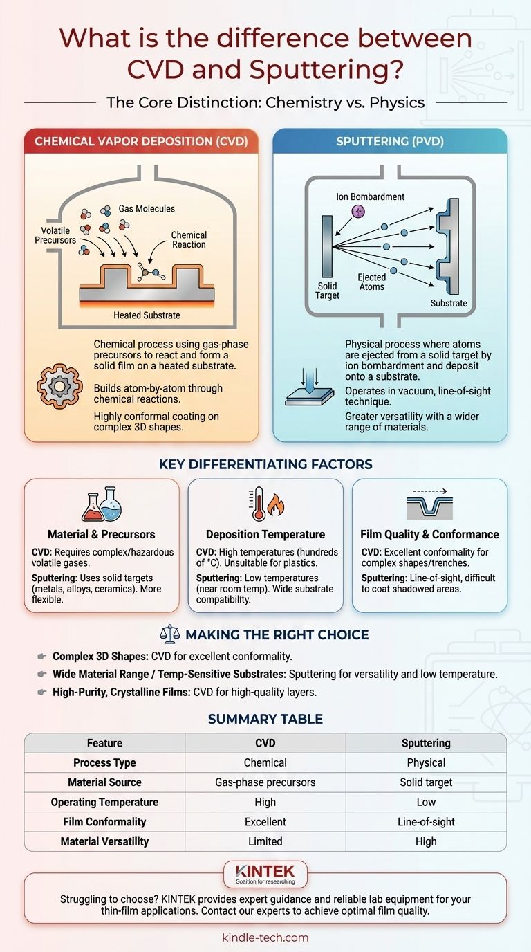
The fundamental difference between CVD and sputtering lies in the state of the material during the deposition process. Chemical Vapor Deposition (CVD) is a chemical process that uses gas-phase precursors to react and form a solid film on a substrate's surface. In contrast, sputtering is a physical process where atoms are ejected from a solid target by high-energy ion bombardment and then deposited onto the substrate.
The choice between CVD and sputtering is a choice between chemistry and physics. CVD builds films atom-by-atom through chemical reactions, offering exceptional uniformity over complex surfaces. Sputtering physically transfers material from a solid source, providing greater versatility with a wider range of materials and lower operating temperatures.
The Core Mechanism: Chemistry vs. Physics
To select the right method, you must first understand how each one works at a fundamental level. One relies on controlled chemical reactions, while the other uses pure physical momentum.
How Chemical Vapor Deposition (CVD) Works
In CVD, volatile precursor gases are introduced into a reaction chamber containing the substrate.
When these gases reach the heated substrate, they undergo a chemical reaction. This reaction decomposes the precursors, leaving behind a solid material that deposits and grows as a thin film on the substrate's surface.
Think of it as precisely controlled condensation, where the "vapor" is a mix of reactive gases that form an entirely new solid material directly on the surface.
How Sputtering (PVD) Works
Sputtering is a form of Physical Vapor Deposition (PVD) and operates in a vacuum.
The process begins with a solid "target" made of the material you wish to deposit. This target is bombarded with high-energy ions, typically from an inert gas like argon.
This bombardment acts like a microscopic billiard game, physically knocking atoms loose from the target. These ejected atoms travel through the vacuum and coat the substrate, building up the thin film.
Key Differentiating Factors
The difference in mechanism leads to significant practical differences in material choice, operating conditions, and the quality of the resulting film.
Material and Precursor Requirements
CVD requires source materials to be available as volatile precursor gases. These can be complex, expensive, or hazardous, limiting the range of depositable materials.
Sputtering is far more flexible. Almost any material that can be formed into a solid target—including pure metals, alloys, and ceramics—can be deposited. It does not require specialized chemical precursors.
Deposition Temperature
CVD processes often require high substrate temperatures (hundreds of degrees Celsius) to provide the energy needed to drive the chemical reactions. This makes it unsuitable for temperature-sensitive substrates like plastics.
Sputtering is generally a low-temperature process. The substrate can remain near room temperature, making it compatible with a much wider variety of materials.
Film Quality and Conformance
CVD excels at producing highly conformal films. Because the chemical reaction occurs everywhere on the exposed surface, it can uniformly coat complex, three-dimensional shapes and deep trenches.
Sputtering is a line-of-sight technique. The sputtered atoms travel in a relatively straight path from the target to the substrate, which can make it difficult to uniformly coat shadowed areas or complex topographies.
Understanding the Trade-offs
Neither method is universally superior. The optimal choice is always dictated by the specific requirements of the application and involves balancing key trade-offs.
The Challenge of CVD: Complexity and Substrates
The primary drawback of CVD is its reliance on precursor chemistry, which can be complex and hazardous. The high temperatures required also severely limit the types of substrates that can be used without being damaged.
The Limitation of Sputtering: Step Coverage
The line-of-sight nature of sputtering is its main limitation. Achieving a uniform, conformal coating over features with high aspect ratios (like deep trenches or around sharp corners) is a significant challenge.
Stress and Film Properties
Both techniques can generate undesirable stress in the film as it forms and cools, potentially impacting performance. However, the high-energy impact of sputtered atoms can sometimes improve film adhesion, while the chemical bonding in CVD often results in very pure, dense films.
Making the Right Choice for Your Application
Your decision depends entirely on your material requirements, the geometry of your substrate, and your desired film properties.
- If your primary focus is coating a complex 3D shape uniformly: CVD is often the superior choice due to its excellent conformality.
- If your primary focus is depositing a wide range of materials, including alloys or ceramics, onto a temperature-sensitive substrate: Sputtering offers unmatched material versatility and low-temperature compatibility.
- If your primary focus is creating high-purity, crystalline films for semiconductors: CVD is the industry standard for its ability to grow exceptionally high-quality layers.
Understanding this core distinction between a chemical reaction and a physical transfer is the key to selecting the most effective deposition technique for your goal.
Summary Table:
| Feature | Chemical Vapor Deposition (CVD) | Sputtering (PVD) |
|---|---|---|
| Process Type | Chemical | Physical |
| Material Source | Gas-phase precursors | Solid target |
| Operating Temperature | High (hundreds of °C) | Low (near room temperature) |
| Film Conformality | Excellent for complex 3D shapes | Line-of-sight, limited for shadowed areas |
| Material Versatility | Limited by precursor availability | High (metals, alloys, ceramics) |
Struggling to choose between CVD and sputtering for your lab's thin-film applications? KINTEK specializes in lab equipment and consumables, providing expert guidance and reliable solutions for all your deposition needs. Whether you require the uniform coatings of CVD or the material versatility of sputtering, our team is here to ensure you achieve optimal film quality and process efficiency. Contact our experts today to discuss your specific requirements and discover the perfect deposition solution for your laboratory!
Visual Guide
Related Products
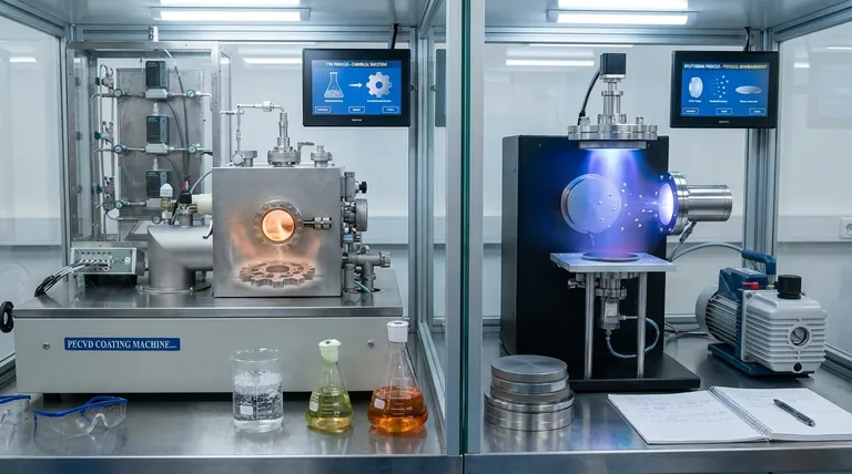
- HFCVD Machine System Equipment for Drawing Die Nano-Diamond Coating
- Custom CVD Diamond Coating for Lab Applications
- Chemical Vapor Deposition CVD Equipment System Chamber Slide PECVD Tube Furnace with Liquid Gasifier PECVD Machine
- Customer Made Versatile CVD Tube Furnace Chemical Vapor Deposition Chamber System Equipment
- Multi Heating Zones CVD Tube Furnace Machine Chemical Vapor Deposition Chamber System Equipment
People Also Ask
- What is the chemical vapor deposition growth process? Build Superior Thin Films from the Atom Up
- What is the specific function of the metal filament in HF-CVD? Key Roles in Diamond Growth
- What types of substrates are used in CVD to facilitate graphene films? Optimize Graphene Growth with the Right Catalyst
- What is the function of tungsten filaments in HFCVD? Powering Diamond Film Synthesis with Thermal Excitation
- What is the full form of HFCVD? A Guide to Hot Filament Chemical Vapor Deposition


