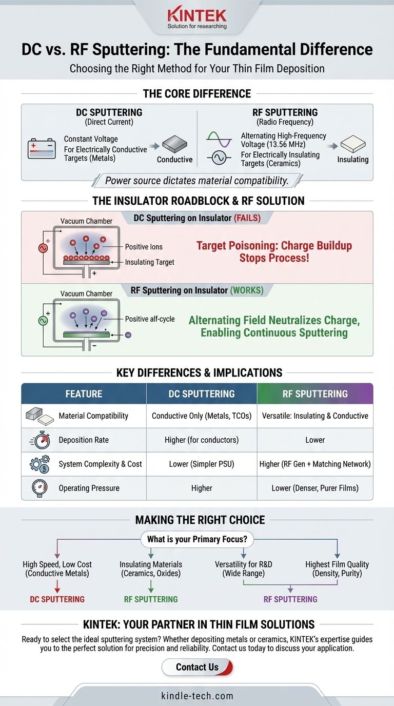
The fundamental difference between DC and RF sputtering lies in the type of power source used, which directly dictates the types of materials that can be deposited. DC (Direct Current) sputtering uses a constant voltage to sputter electrically conductive targets, while RF (Radio Frequency) sputtering uses an alternating high-frequency voltage, making it possible to sputter electrically insulating targets.
The core decision between DC and RF sputtering is not about which method is superior, but which is compatible with your target material's electrical properties. DC is a simple, fast, and efficient process for metals, while RF is the essential solution for insulators, preventing a process-killing charge buildup on the target surface.
The Problem of Charge: Why Both Methods Exist
The need for two distinct sputtering methods comes down to a simple electrical problem: what happens when you bombard an insulating surface with positive ions.
How DC Sputtering Works
In a standard DC system, a high negative DC voltage is applied to the target material, which acts as a cathode. This creates a plasma of positively charged ions (typically argon) that are aggressively accelerated toward the negatively charged target.
The energetic impact of these ions physically knocks atoms off the target material, which then travel through the vacuum chamber to coat your substrate. This process is continuous and efficient as long as the target is conductive, allowing the positive charge from the ions to be neutralized.
The Insulator Roadblock
If you attempt to use DC sputtering with a non-conductive (insulating) target like a ceramic, the process quickly fails. Positive ions strike the target surface and their charge accumulates because the insulating material cannot conduct it away.
This buildup of positive charge on the target surface, known as target poisoning or charging, creates a positive potential that repels the incoming positive ions from the plasma. This effectively stops the sputtering process and can lead to damaging electrical arcs.
The RF Sputtering Solution
RF sputtering overcomes this challenge by using a high-frequency alternating voltage, typically fixed at 13.56 MHz. This alternating field makes the target rapidly switch between being negatively and positively charged.
During the negative half of the cycle, the target attracts positive ions, causing sputtering just like in a DC system. Crucially, during the positive half of the cycle, the target attracts electrons from the plasma. These electrons flood the surface and neutralize the positive charge that accumulated during the previous half-cycle. This rapid switching prevents charge buildup, allowing for the continuous, stable sputtering of insulating materials.
Practical Implications and Key Differences
The choice between DC and a RF power source has several direct consequences for the sputtering process.
Material Compatibility
This is the most critical distinction. DC sputtering is restricted to electrically conductive materials like metals and transparent conductive oxides.
RF sputtering is highly versatile, capable of depositing insulating materials such as ceramics (e.g., aluminum oxide, silicon dioxide) and other dielectrics. It can also deposit conductive materials, though often less efficiently than DC.
Deposition Rate
For a given material that can be sputtered by both methods (i.e., a metal), DC sputtering generally offers a higher deposition rate. This is because the power is continuously dedicated to accelerating ions for sputtering.
In RF sputtering, a portion of each cycle is used for electron bombardment to neutralize charge, not for sputtering, which results in a comparatively lower deposition rate.
System Complexity and Cost
DC sputtering systems are simpler and more cost-effective. They consist of a straightforward high-voltage DC power supply.
RF systems are more complex and expensive. They require a specialized RF power generator and an impedance matching network to ensure that the RF power is efficiently transferred to the plasma rather than being reflected back to the source.
Operating Pressure
RF energy is more efficient at sustaining a plasma. Consequently, RF sputtering can operate at lower gas pressures (often below 15 mTorr) than DC sputtering.
Operating at lower pressure increases the mean free path of the sputtered atoms. This reduces the chance of them colliding with gas molecules on their way to the substrate, which can result in purer, denser, and higher-quality thin films.
Making the Right Choice for Your Application
Ultimately, the correct technology is determined by your specific material and performance requirements.
- If your primary focus is depositing conductive materials (metals) at high speed and low cost: DC sputtering is the clear and more efficient choice.
- If your primary focus is depositing insulating or dielectric materials (ceramics, oxides): RF sputtering is the only viable option to prevent target charging.
- If your primary focus is versatility for research and development on a wide range of materials: An RF sputtering system provides the greatest flexibility, as it can deposit both insulators and conductors.
- If your primary focus is achieving the highest possible film density and purity: RF sputtering's ability to operate at lower pressures can provide a distinct advantage.
Your choice is dictated by the fundamental electrical properties of your source material and your desired film characteristics.
Summary Table:
| Feature | DC Sputtering | RF Sputtering |
|---|---|---|
| Material Compatibility | Conductive materials (Metals) | Insulating & Conductive materials (Ceramics, Oxides, Metals) |
| Deposition Rate | Higher for conductive materials | Lower |
| System Complexity & Cost | Lower | Higher (requires RF generator & matching network) |
| Operating Pressure | Higher | Lower (results in denser, purer films) |
| Primary Use Case | Fast, cost-effective metal deposition | Essential for insulators; versatile for R&D |
Ready to select the ideal sputtering system for your lab's thin film needs?
Whether you are depositing conductive metals or insulating ceramics, KINTEK's expertise in lab equipment can guide you to the perfect solution. Our sputtering systems are designed to deliver precision, reliability, and the high-quality results your research demands.
Contact us today using the form below to discuss your specific application and discover how KINTEK can enhance your laboratory's capabilities.
Visual Guide
Related Products
- Lab Sterile Slapping Type Homogenizer for Tissue Mashing and Dispersing
- Spark Plasma Sintering Furnace SPS Furnace
- Single Punch Manual Tablet Press Machine TDP Tablet Punching Machine
People Also Ask
- How does a laboratory automatic masticator or homogenizer facilitate the processing of biofilm samples? Optimize Accuracy
- How do ultrasonic cell disruptors or dispersion equipment function during ZIF-8 synthesis? Master Acoustic Cavitation
- What is the primary function of an ultrasonic cleaner in coating? Achieve Unmatched Substrate Purity for PVD Adhesion
- What role does a laboratory homogenizer play in radioactive cesium detection? Ensure Accuracy in Wildlife Sampling
- How does a homogenizer affect the quality of electrode slurry? Master Battery Consistency with High-Shear Mixing


