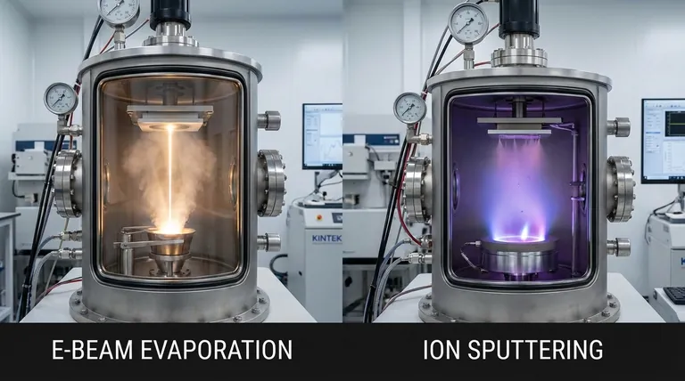
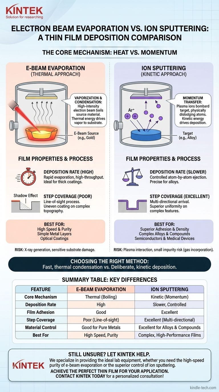
At its core, the difference between electron beam evaporation and ion sputtering is the physics used to move material from a source to your substrate. E-beam evaporation is a thermal process that uses a focused beam of electrons to boil a source material, creating a vapor that condenses onto the substrate. Ion sputtering is a kinetic process that uses a plasma to accelerate gas ions, which then physically knock atoms off a source target like microscopic billiard balls.
Choosing between these methods is not a question of which is "better," but which is precisely suited to your goal. Evaporation excels at high-speed, high-purity deposition for simpler structures, while sputtering provides superior control, density, and adhesion for complex, high-performance films.
The Core Mechanism: Heat vs. Momentum
Understanding how each process liberates atoms from the source material is the key to understanding all subsequent differences in film quality and application.
How E-Beam Evaporation Works (The Thermal Approach)
In an e-beam system, a high-intensity electron beam is generated and magnetically guided to strike a source material (like gold or titanium) held in a crucible inside a high-vacuum chamber.
This intense energy transfer rapidly heats the material past its melting and boiling points, causing it to evaporate (or sublime).
These vaporized atoms travel in a straight, line-of-sight path until they hit the cooler substrate, where they condense to form a thin film. The energy of these arriving atoms is relatively low, dictated by thermal energy (typically 0.1-0.5 eV).
How Ion Sputtering Works (The Kinetic Approach)
Sputtering begins by introducing an inert gas, almost always Argon, into the vacuum chamber and creating a plasma.
An electric field accelerates the positive Argon ions from the plasma, causing them to bombard a "target" made of the desired coating material.
This collision is a pure momentum transfer event. The impact has enough force to dislodge or "sputter" atoms from the target. These ejected atoms have much higher kinetic energy (1-10 eV) and travel through the chamber to deposit onto the substrate.
Key Differences in Process and Film Quality
The fundamental difference between a thermal and a kinetic process leads to significant and predictable variations in the final thin film.
Film Adhesion and Density
Sputtering produces films with significantly better adhesion and higher density. The higher kinetic energy of the sputtered atoms allows them to impact the substrate surface with enough force to improve bonding and arrange themselves into a denser, more tightly packed structure.
Evaporated films, formed from lower-energy atoms gently condensing, are often more porous and have weaker adhesion to the substrate.
Deposition Rate
E-beam evaporation generally offers much higher deposition rates. It is capable of evaporating large volumes of material very quickly, making it highly efficient for thick coatings or high-throughput manufacturing, such as in optical lens coating.
Sputtering is a slower, more deliberate process, as atoms are ejected one by one through bombardment.
Step Coverage and Uniformity
Sputtering provides superior "step coverage," meaning it can more uniformly coat surfaces with complex topography, like trenches in a semiconductor wafer. The higher chamber pressure and scattering events mean atoms arrive at the substrate from multiple angles.
E-beam evaporation is a strict line-of-sight process. Any part of the substrate in a "shadow" relative to the source will not get coated, leading to poor step coverage.
Process Control
Sputtering allows for extremely precise control over film thickness and composition. The deposition rate is stable and directly related to the power applied to the target. This makes it ideal for depositing complex alloys or compounds where maintaining stoichiometry is critical.
Controlling the rate of evaporation in an e-beam system can be more challenging, as it's sensitive to the beam's position and power fluctuations.
Understanding the Trade-offs and Limitations
Neither technology is a universal solution. Understanding their inherent drawbacks is critical for making an informed choice.
Material Compatibility
E-beam evaporation excels at depositing materials with very high melting points, like refractory metals and ceramics, which can be difficult to sputter effectively.
Sputtering is more versatile for creating films from alloys or compounds. You can use a pre-alloyed target or co-sputter from multiple targets to achieve a desired composition with high precision.
Substrate Damage and Heating
The intense electron beam generates secondary radiation, including X-rays, which can damage sensitive electronic components or polymers. There is also significant radiant heat from the molten source material.
Sputtering involves direct plasma interaction with the substrate, which can cause some surface damage from ion bombardment. The plasma also contributes to substrate heating.
Purity and Contamination
E-beam evaporation can produce films of very high purity because only the source material is heated, minimizing outgassing from the chamber walls.
Sputtered films run a small risk of having the sputtering gas (e.g., Argon) incorporated into the film structure, which can alter its properties.
Making the Right Choice for Your Application
Your choice should be dictated entirely by the required properties of your final thin film.
- If your primary focus is high deposition speed for optical coatings or simple metal layers: E-beam evaporation is often the most cost-effective and efficient method.
- If your primary focus is exceptional film adhesion, density, and uniformity for semiconductors, hard coatings, or medical devices: Sputtering is the definitive choice for high-performance applications.
- If you need to maintain the precise composition of a complex alloy or compound material: Sputtering offers far superior control and repeatability.
- If you must coat a complex surface with features like trenches or vias: Sputtering's ability to coat from multiple angles gives it a distinct advantage in step coverage.
Ultimately, your decision rests on understanding that you are choosing between a fast, thermal condensation process and a deliberate, high-energy kinetic deposition process.
Summary Table:
| Feature | E-Beam Evaporation | Ion Sputtering |
|---|---|---|
| Core Mechanism | Thermal (Boiling by electron beam) | Kinetic (Momentum transfer from ion bombardment) |
| Best For | High speed, high purity, simple coatings | Superior adhesion, density, complex coatings |
| Deposition Rate | High | Slower, more controlled |
| Film Adhesion | Good | Excellent |
| Step Coverage | Poor (Line-of-sight) | Excellent (Multi-directional) |
| Material Control | Good for pure metals | Excellent for alloys & compounds |
Still unsure which deposition method is right for your project? The experts at KINTEK are here to help. We specialize in providing the ideal lab equipment, whether you need the high-speed purity of an e-beam evaporation system or the superior control of an ion sputtering system for semiconductors, medical devices, or advanced research. Let us help you achieve the perfect thin film for your application.
Contact KINTEK today for a personalized consultation!
Visual Guide
Related Products
- Electron Beam Evaporation Coating Tungsten Crucible and Molybdenum Crucible for High Temperature Applications
- Electron Beam Evaporation Coating Oxygen-Free Copper Crucible and Evaporation Boat
- Electron Beam Evaporation Coating Gold Plating Tungsten Molybdenum Crucible for Evaporation
- Electron Beam Evaporation Coating Conductive Boron Nitride Crucible BN Crucible
- E Beam Crucibles Electron Gun Beam Crucible for Evaporation
People Also Ask
- What materials are used in electron beam evaporation? Master High-Purity Thin Film Deposition
- What is the container that holds the metal source material called in e-beam evaporation? Ensure Purity and Quality in Your Thin-Film Deposition
- What are the applications of e-beam evaporation? Achieve High-Purity Coatings for Optics & Electronics
- What is the deposition rate of e-beam evaporation? Control Thin Film Quality and Speed
- What is the process of e-beam coating? Achieve High-Purity, Precise Thin Films for Your Lab


