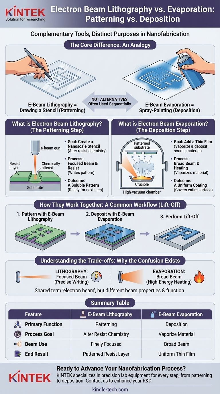
At their core, electron beam evaporation and electron beam lithography are fundamentally different processes used for entirely different purposes in nanofabrication. Electron beam lithography is a patterning technique used to draw a nanoscale design, while electron beam evaporation is a deposition technique used to coat a surface with a thin film of material. They are not alternatives; they are often used sequentially to create a final device.
The simplest way to understand the difference is with an analogy: Electron beam lithography is like drawing a stencil, while electron beam evaporation is like spray-painting over that stencil to fill in the design. One creates the pattern, the other adds the material.
What is Electron Beam Lithography? (The Patterning Step)
Electron beam (e-beam) lithography is a method for creating extremely small patterns on a surface. Its primary function is to define where material should or should not be in a subsequent step.
The Goal: Creating a Nanoscale Stencil
The objective of e-beam lithography is not to add or remove material itself, but to alter the chemical properties of a special coating called a resist. This creates a template for later processing.
The Process: A Focused Beam and a Resist
First, a substrate (like a silicon wafer) is coated with a thin layer of an electron-sensitive polymer, the resist. A highly focused, computer-controlled beam of electrons then scans across the surface, drawing a pattern by exposing specific areas of this resist.
The Outcome: A Soluble Pattern
The electron beam changes the chemical structure of the resist, making the exposed areas either more or less soluble in a developer solvent. After development, a patterned stencil of resist is left behind on the substrate, ready for the next fabrication step.
What is Electron Beam Evaporation? (The Deposition Step)
Electron beam (e-beam) evaporation is a type of Physical Vapor Deposition (PVD). Its sole purpose is to deposit a thin, uniform layer of a source material onto a substrate.
The Goal: Adding a Thin Film of Material
The objective is to take a solid source material, such as gold, titanium, or silicon dioxide, and turn it into a vapor that coats everything inside a vacuum chamber, including your patterned substrate.
The Process: Vaporizing a Source Material
Inside a high-vacuum chamber, a high-energy electron beam is generated from a hot tungsten filament. Magnetic fields steer and focus this beam onto a crucible containing the source material. The intense energy from the beam heats the material until it melts and evaporates (or sublimates).
The Outcome: A Uniform Coating
These vaporized atoms travel in straight lines through the vacuum, eventually landing on and sticking to the substrate, which is placed above the source. This results in a thin, uniform film of the material covering the entire surface.
How They Work Together: A Common Workflow
To resolve the core confusion, it is critical to see how these two processes are used together in a common technique called lift-off.
Step 1: Pattern with E-Beam Lithography
You start with a substrate coated in resist and use e-beam lithography to create your desired pattern in that resist layer. This leaves behind a polymer stencil.
Step 2: Deposit with E-Beam Evaporation
The patterned substrate is then placed in an e-beam evaporator. A thin film of metal (e.g., gold) is deposited over the entire surface, coating both the top of the resist stencil and the exposed substrate areas.
Step 3: Perform Lift-Off
Finally, the substrate is placed in a solvent that dissolves the remaining resist. As the resist stencil washes away, it takes the metal that was on top of it with it, "lifting off" the unwanted material.
This leaves behind only the metal that was directly deposited on the substrate, perfectly matching the pattern originally drawn with the electron beam.
Understanding the Trade-offs: Why the Confusion Exists
The confusion between these two techniques is understandable, as both use the term "electron beam." However, the properties and function of the beam in each process are completely different.
The Common Element: The Electron Beam
Both processes use a beam of electrons as their primary tool. This shared terminology is the main source of the misunderstanding.
Different Beam Properties: Focused vs. Broad
In lithography, the beam is extremely narrow and finely focused (a few nanometers wide) to "write" with high precision. In evaporation, the beam is much broader and is used as a powerful heat source to melt a large area of source material.
Different Purposes: Writing vs. Heating
The purpose of the beam in lithography is to deliver a precise dose of energy to change a polymer's chemistry. The purpose of the beam in evaporation is to deliver a massive amount of thermal energy to vaporize a bulk material.
Making the Right Choice for Your Goal
Selecting the right process depends entirely on what you are trying to accomplish in your fabrication workflow.
- If your primary focus is creating a high-resolution pattern: You must use electron beam lithography to define the features on your resist-coated substrate.
- If your primary focus is depositing a high-purity, high-melting-point material: Electron beam evaporation is an excellent choice for creating your thin film.
- If your primary focus is creating a final, patterned nanostructure: You will use both techniques, starting with lithography to create the stencil and following with evaporation and lift-off to form the structure.
Ultimately, these are not competing technologies but complementary tools in the nanofabrication toolkit, each perfectly designed for a specific step in creating microscopic devices.
Summary Table:
| Feature | Electron Beam Lithography | Electron Beam Evaporation |
|---|---|---|
| Primary Function | Patterning (creates a nanoscale stencil) | Deposition (adds a thin film of material) |
| Process Goal | Alter resist chemistry to define patterns | Vaporize and deposit source material |
| Beam Use | Finely focused for high-precision writing | Broad beam for high-energy heating |
| Common Application | Creating the initial design template | Coating the substrate with material |
| End Result | Patterned resist layer on substrate | Uniform thin film on substrate |
Ready to Advance Your Nanofabrication Process?
Understanding the distinct roles of patterning and deposition is crucial for successful device fabrication. Whether you are defining intricate patterns with lithography or depositing high-purity thin films, having the right equipment is key.
KINTEK specializes in precision lab equipment and consumables, serving the exacting needs of nanotechnology and materials science laboratories. Our range of solutions supports every step of your workflow, from initial patterning to final deposition.
Let us help you achieve superior results:
- High-resolution patterning systems for defining your nanoscale designs.
- Reliable evaporation systems for depositing high-quality, uniform thin films.
- Expert support and consumables to keep your lab running efficiently.
Contact us today to discuss how our equipment can enhance your research and development. Our experts are ready to help you select the perfect tools for your specific application.
Get in touch with our team now →
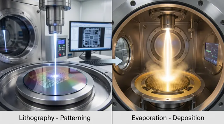
Visual Guide