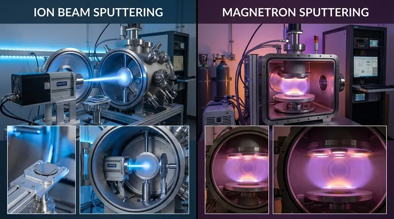
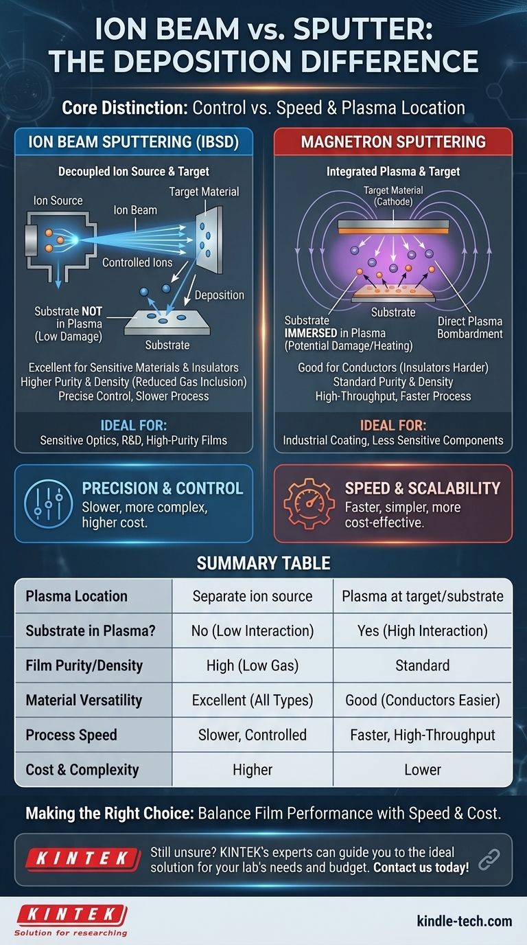
At its core, the difference between ion beam and sputter deposition lies in the location of the plasma and its relationship to the material target. Ion beam sputtering decouples the ion source from the target, creating a controlled beam of ions, while conventional magnetron sputtering generates a plasma directly between the target and the substrate.
The fundamental distinction is control versus speed. Ion beam sputtering separates the plasma source from the target, offering unparalleled control and making it ideal for sensitive materials. Magnetron sputtering integrates them, creating a faster, more direct process where the substrate is immersed in plasma.
The Core Architectural Difference: Source and Target
To understand the practical outcomes of each method, we must first examine their fundamental design. The key is whether the process that creates ions is combined with the material being sputtered.
How Magnetron Sputtering Works
In magnetron sputtering, the target (the material to be deposited) also acts as the cathode. An inert gas is introduced, and a strong voltage is applied, creating a plasma that is confined between the target and the substrate by a magnetic field. Ions from this plasma directly bombard the target, dislodging atoms that then coat the substrate.
How Ion Beam Sputtering Works
Ion beam sputter deposition (IBSD) uses a completely separate, dedicated ion source. This source generates a well-defined, focused beam of ions that is aimed at the target material. The target is physically separate and electrically neutral. The ion beam strikes the target, sputtering atoms that then travel to coat the substrate.
Key Implications of This Difference
This architectural separation has profound consequences for the deposition process, film quality, and the types of materials that can be used.
The Role of Plasma
The most critical difference is that in ion beam sputtering, the substrate is not exposed to plasma. The plasma is safely contained within the ion source. In magnetron sputtering, the substrate is directly immersed in the energetic plasma environment, which can cause heating and unwanted interactions.
Substrate and Material Versatility
Because there is no plasma between the target and substrate in IBSD, there is no need for a target bias. This makes the process ideal for depositing films onto sensitive substrates (like delicate electronics or optics) and for sputtering both conducting and insulating materials with ease.
Film Purity and Density
The controlled, high-energy nature of the ion beam results in a more ordered deposition. This significantly reduces the inclusion of inert sputter gas in the final film, leading to higher purity and density compared to the more chaotic environment of magnetron sputtering.
Understanding the Trade-offs
Neither method is universally superior; the choice depends entirely on the application's specific requirements.
Precision vs. Speed
Ion beam sputtering offers independent control over ion energy and current, allowing for the precise tuning of film properties like stress and density. Magnetron sputtering is generally a much faster process, making it better suited for high-volume industrial applications where throughput is critical.
Complexity and Cost
The dedicated ion source makes IBSD systems more complex and expensive to build and operate. Magnetron sputtering systems are simpler, more common, and typically more cost-effective for large-scale coating operations.
Making the Right Choice for Your Goal
Your application's priorities will dictate the correct method.
- If your primary focus is high-quality, dense films for sensitive optics or advanced electronics: Ion beam sputtering is the superior choice for its precision, purity, and low-damage process.
- If your primary focus is high-throughput, cost-effective coating of less sensitive components: Magnetron sputtering is the industry standard due to its speed and scalability.
- If your primary focus is maximum versatility for R&D on diverse materials: Ion beam sputtering offers more straightforward processing for both insulators and conductors with fewer process complications.
Ultimately, choosing between these techniques is a strategic decision based on balancing film performance requirements with manufacturing speed and cost.
Summary Table:
| Feature | Ion Beam Sputtering | Magnetron Sputtering |
|---|---|---|
| Plasma Location | Separate ion source | Plasma at target/substrate |
| Substrate in Plasma? | No | Yes |
| Film Purity/Density | High (low gas inclusion) | Standard |
| Material Versatility | Excellent (conductors & insulators) | Good (conductors easier) |
| Process Speed | Slower, more controlled | Faster, high-throughput |
| Cost & Complexity | Higher | Lower |
| Ideal For | Sensitive optics, R&D, high-purity films | Industrial coating, less sensitive components |
Still unsure which deposition method is right for your project? The experts at KINTEK are here to help. We specialize in lab equipment and consumables, offering deep technical knowledge in thin-film deposition technologies. Whether you require the ultimate precision of ion beam sputtering for sensitive R&D or the high-throughput capabilities of magnetron sputtering for production, we can guide you to the ideal solution for your laboratory's specific needs and budget.
Contact KINTEK today to discuss your application and discover how our expertise can enhance your lab's capabilities and ensure your project's success.
Visual Guide
Related Products
- Electron Beam Evaporation Coating Oxygen-Free Copper Crucible and Evaporation Boat
- Electron Beam Evaporation Coating Gold Plating Tungsten Molybdenum Crucible for Evaporation
- Chemical Vapor Deposition CVD Equipment System Chamber Slide PECVD Tube Furnace with Liquid Gasifier PECVD Machine
- Molybdenum Tungsten Tantalum Evaporation Boat for High Temperature Applications
- Electron Beam Evaporation Coating Conductive Boron Nitride Crucible BN Crucible
People Also Ask
- What is e-beam evaporation? Achieve High-Purity Thin Film Deposition for Your Lab
- What are the applications of electron beams? From Nanoscale Imaging to Industrial Manufacturing
- What is the voltage of e-beam evaporation? Achieve Precise Thin-Film Deposition
- What is the current of e-beam evaporation? A Guide to High-Purity Thin Film Deposition
- What is the deposition rate of e-beam evaporation? Control Thin Film Quality and Speed


